The JTM1607 is N-channel MOS Field Effect Transistor designe
时间:2015-10-14 09:05来源:未知 作者:oumao18 点击:
次
目录 1. 产品概述 2. 产品特点 3. 应用范围 4. 下载产品资料PDF文档 5. 产品封装图 6. 电路原理图 7. 功能概述 8 . 相关产品 一 , 产品概述( General Description) The JTM1607 is N-channel MOS Field Effect Transistor
|
目录
一,产品概述(General Description)
The JTM1607 is N-channel MOS Field Effect Transistor designed for
high current switching applications. Rugged EAS capability and ultra low
RDS(ON) is suitable for PWM.
二.产品特点(Features)
VDS=75V; ID=150A@ VGS=10V;
RDS(ON)<6.3mΩ @ VGS=10V
Ultra Low On-Resistance
High UIS and UIS 100% Test
三,应用范围 (Applications)
Hard Switched and High Frequency Circuits
Uninterruptible Power Supply
四.下载产品资料PDF文档
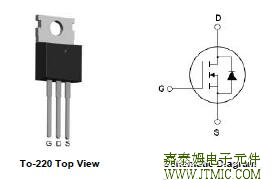
五,产品封装图 (Package)
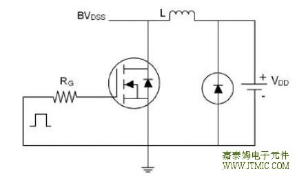
六.电路原理图
七,功能概述
Table 1. Absolute Maximum Ratings (TA=25℃)
|
Symbol |
Parameter |
Value |
Unit |
|
VDS |
Drain-Source Voltage (VGS=0V) |
75 |
V |
|
VGS |
Gate-Source Voltage (VDS=0V) |
±25 |
V |
|
ID (DC) |
Drain Current (DC) at Tc=25℃ |
150 |
A |
|
ID (DC) |
Drain Current (DC) at Tc=100℃ |
115 |
A |
|
IDM (pluse) |
(Note 1)
Drain Current-Continuous@ Current-Pulsed |
600 |
A |
|
PD |
Maximum Power Dissipation(Tc=25℃) |
380 |
W |
|
|
Derating Factor |
2.5 |
W/℃ |
|
EAS |
(Note 2)
Single Pulse Avalanche Energy |
1000 |
mJ |
|
TJ,TSTG |
Operating Junction and Storage Temperature Range |
-55 To 175 |
℃ |
(责任编辑:oumao18) |
------分隔线----------------------------


 粤ICP备13004986号-3