|
目录
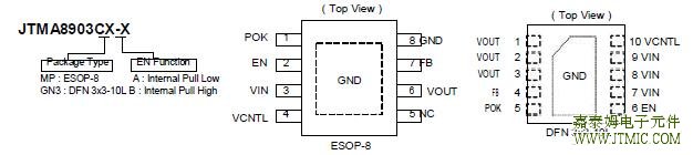
一,产品概述(General Description) The JTMA8903C series is a 3A ultra low dropout linear regulator. This product is specifically designed to provide well supply voltage for front-side-bus termination on motherboards and NB applications. The IC needs two supply voltages, a control voltage for the circuitry and a main supply voltage for power conversion, to reduce power dissipation and provide extremely low dropout. The JTMA8903C series integrates many functions. A Power-On- Reset (POR) circuit monitors both supply voltages to prevent wrong operations. A thermal shutdown and current limit functions protect the device against thermal and current over-loads. A POK indicates the output status with time delay which is set internally. It can control other converter for power sequence. The JTMA8903C series can be enabled by other power system. Pulling and holding the EN pin below 0.4V shuts off the output. The JTMA8903C series is available in DFN 3x3-10L & ESOP-8 package which features small size as SO-8 and an Exposed Pad to reduce the junction-to-case resistance. 二.产品特点(Features) Ultra Low Dropout 0.21V(typical) @ 2A Output Current for 1.2V Output Voltage Low ESR Output Capacitor (Multi-layer Chip Capacitors (MLCC)) Applicable EN Pull-low for JTMA8903CMP-A EN Pull-high for JTMA8903CMP-B Fast Transient Response Adjustable Output Voltage by External Resistors Power-On-Reset Monitoring on Both VCNTL and VIN Pins Internal Soft-Start Current-Limit and Thermal Shutdown Protection Power-OK Output with a Delay Time SO-8 with Exposed Pad Pb-Free & DFN 3x3-10L Package. Halogen Free Product 三,应用范围 (Applications) 四.技术规格书下载(产品PDF)
 六.电路原理图 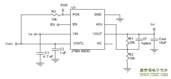 七,功能概述
CNTL Supply Voltage (VCNTL) --------------------------- -0.3V To 6.5V
Input Supply Voltage (VIN) ------------------------------- -0.3V To 6.5V EN & FB Pin Voltage (VEN/VFB) ------------------------- -0.3V To VCNTL+0.3V Power Good Voltage (VPOK) ---------------------------- -0.3V To 6.5V Power Dissipation (PD) ---------------------------------- 2.5W Storage Temperature Range (TST) -------------------- -65°C To 150°C Junction Temperature Range (TJ) --------------------- -40°C To 150°C Thermal Resistance Junction to Ambient (Rth ja)Note. ESOP-8 ------- 40°C/W
DFN 3x3-10L
ESOP-8 ------- 15°C/WThermal Resistance Junction to Case (Rth jc)Note 62.5°C/W DFN 3x3-10L 17°C/W 八,相关芯片选择指南
(责任编辑:oumao18) |


 粤ICP备13004986号-3