产品封装图 (Package)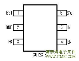 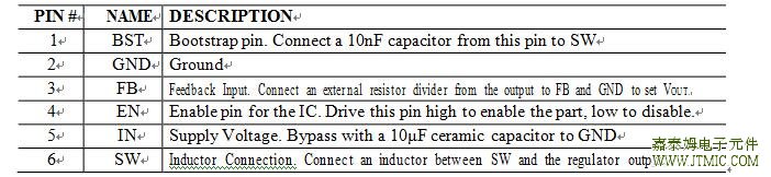 六.电路原理图 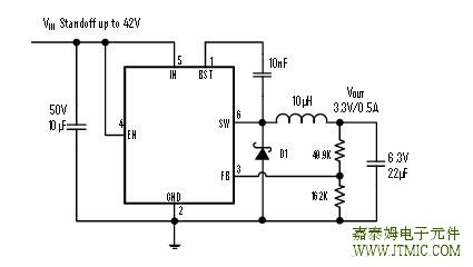 七,功能概述 Loop Operation The JTM2459 is a wide input range, high-efficiency, DC-to-DC step-down switching regulator, capable of delivering up to 1.5A of output current, integrated with a 300mΩ high side MOSFET. It uses a PWM current-mode control scheme. An error amplifier integrates error between the FB signal and the internal reference voltage. The output of the integrator is then compared to the sum of a current-sense signal and the slope compensation ramp. This operation generates a PWM signal that modulates the duty cycle of the power MOSFETs to achieve regulation for output voltage. Light Load Operation Traditionally, a fixed constant frequency PWM DC-DC regulator always switches even when the output load is small. When energy is shuffling back and forth through the power MOSFETs, power is lost due to the finite RDSONs of the MOSFETs and parasitic capacitances. At light load, this loss is prominent and efficiency is therefore very low. JTM2459 employs a proprietary control scheme that improves efficiency in this situation by enabling the device into a power save mode during light load, thereby extending the range of high efficiency operation. Setting Output Voltages Output voltages are set by external resistors. The FB threshold is 0.8V. RTOP = RBOTTOM x [(VOUT / 0.8) - 1] Inductor Selection The peak-to-peak ripple is limited to 30% of the maximum output current. This places the peak current far enough from the minimum overcurrent trip level to ensure reliableoperation while providing enough current ripples for the current mode converter to operate stably. In this case, for 1.5A maximum output current, the maximum inductor ripple current is 500 mA. The inductor size is estimated as following equation: LIDEAL=(VIN(MAX)-VOUT)/IRIPPLE*DMIN*(1/FOSC) Therefore, for VOUT=5V, The inductor values is calculated to be L = 13μH. Chose 10μH or 15μH For VOUT =3.3V, The inductor values is calculated to be L = 9.2μH.Chose 10μH Output Capacitor Selection For most applications a nominal 22μF or larger capacitor is suitable. The JTM2459 internal compensation is designed for a fixed corner frequency that is equal to FC= = 8.7Khz √ For example, for VOUT=5V, L=15μH, COUT=22μF. The output capacitor keeps output ripple small and ensures control-loop stability. The output capacitor must also have low impedance at the switching frequency. Ceramic, polymer, and tantalum capacitors are suitable, with ceramic exhibiting the lowest ESR and high-frequency impedance. Output ripple with a ceramic output capacitor is approximately as follows: VRIPPLE = IL(PEAK)[1 / (2π x fOSC x COUT)] If the capacitor has significant ESR, the output ripple component due to capacitor ESR is as follows: VRIPPLE(ESR) = IL(PEAK) x ESR Input Capacitor Selection The input capacitor in a DC-to-DC converter reduces current peaks drawn from the battery or other input power source and reduces switching noise in the controller. The impedance of theinput capacitor at the switching frequency should be less than that of the input source so high-frequency switching currents do not pass through the input source. The output capacitor keeps output ripple small and ensures control-loop stability. 八,相关产品
(责任编辑:oumao18) |
||||||||||||||||||||||||||||||||||||||||||||||||||||||||||||||||||||||||||||||||||||||||||||||||||||||||||||||||||||||||||||||||||||||||||||||||||||||||||||||||||||||||||||||||||||||||||||||||||||||||||||||||||||||||||||||||||||||||||||||||||||||||||||||||||||||||||||||||||||||||||||||||||

 粤ICP备13004986号-3