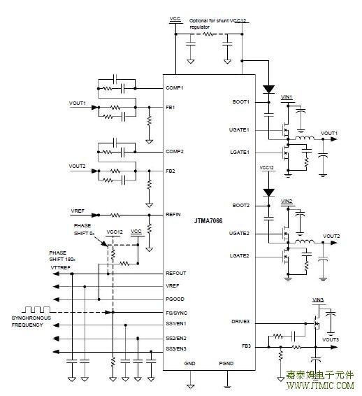
 七,功能概述 Soft-Start/Enable The three SS/EN pins control the soft-start and enable or disable the controller. In Independent mode, the three regulators all have independent soft-start and enable functions. Connect a soft-start capacitor from each SS/EN pin to the GND to set the soft-start interval, and an open drain logic signal for each SS/EN pin will enable or dis- able the respective output. Figure 4. Shows the soft-start interval. When both VCC and VCC12 reach their Power-On-Reset threshold 4.23V and 7.8V, a 30µA current source starts to charge the capacitor. When the SS reaches the enabled threshold about 1V, the internal 0.6V reference starts to rise and follows the SS; the error amplifier output (COMP) sud- denly raises to 1.1V, which is the valley of the oscillator’s triangle wave, leads the VOUT to start up. Until the SS reaches about 3.0V, the internal reference completes the soft-start interval and reaches to 0.6V; then VOUT1 is in regulation. PGOOD The PGOOD output is an open-drain device, when the VCC is present; the gate of open-drain device will be high, forcing the PGOOD pin to go low. The three SS/EN pins and the SCP signals control the PGOOD signal (see block diagram), after the three SS/EN signals are over threshold high 3.3V and three outputs have no short- circuit, the PGOOD goes high to indicate all regulators are ready. If any of the SS/EN pins goes below threshold low 3.2V, the PGOOD will go low. Also, if any of the outputs has a short, the PGOOD pull low and if short-circuit condi- tion continues for 1-2 clock pulses, all regulators will shut down. If the short-circuit is not long enough to shut down, it may still cause PGOOD to go low momentarily. Because the PGOOD is an open-drain device, the typical range of the value to connect a pull high resistor to VCC will be 1kΩ to 10kΩ; if PGOOD is not used, leave it open. Shunt Regulator The JTMA7066 must have two power supplies VCC (5V) and VCC12 (12V) to drive the IC; VCC (5V) is for the con- trol circuit and VCC12 (12V) is for the drivers of outputs.But it can also operate only VCC12, because the shunt (责任编辑:oumao18) |
|||||||||||||||||||||||||

 粤ICP备13004986号-3