The JTM9905,JTM9904 Series product is a high integration sol
时间:2015-08-21 12:49来源:未知 作者:oumao18 点击:
次
GENERAL DESCRIPTION The JTM9905 Series product is a high integration solution for lithium- ion/polymer battery protection. JTM9905 contains advanced power MOSFET, high-accuracy voltage detection circuits and delay circuits. JTM9905 is put i
GENERAL DESCRIPTION
The JTM9905 Series product is a high integration solution for lithium-
ion/polymer battery protection.
JTM9905 contains advanced power MOSFET, high-accuracy voltage
detection circuits and delay circuits.
JTM9905 is put into an SOP8-PP package and only one external
component makes it an ideal solution in limited space of battery pack.
JTM9905 has all the protection functions required in the battery application including
overcharging, overdischarging, overcurrent and load short circuiting protection etc. The
accurate overcharging detection voltage ensures safe and full utilization charging.
The low standby current drains little current from the cell while in storage.
The device is not only targeted for digital cellular phones, but also for any other
Li-Ion and Li-Poly battery-powered information appliances requiring long-
term battery life.
FEATURES
Protection of Charger Reverse
Connection
Protection of Battery Cell Reverse
Connection
· Integrate Advanced Power MOSFET
with Equivalent of 8.5mΩ RDS(ON)
· sop-pp package
Only one External Capcitor Required
· Over-temperature Protection
· Overcharge Current Protection
· Two-step Overcurrent Detection:
-Overdischarge Current
-Load Short Circuiting
· Charger Detection Function
· 0V Battery Charging Function
- Delay Times are generated inside
· High-accuracy Voltage Detection
· Low Current Consumption
- Operation Mode:7μ A typ.
- Power-down Mode: 4μ A typ.
· RoHS Compliant and Lead (Pb) Free
APPLICATIONS
One-Cell Lithium-ion Battery Pack
Lithium-Polymer Battery Pack
Power Bank
PIN CONFIGURATION
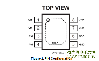
JTM9905 PIN
NUMBER |
PIN NAME |
PIN DESCRIPTION |
|
1,2,3,4 |
VM |
The negative terminal of the battery pack. The internal FET switch
connects this terminal to GND |
|
5,7,8 |
GND |
Ground, connect the negative terminal of the battery to this pin |
|
6 |
VDD |
Power Supply |
|
9 |
EPAD |
Exposed pad,Must connect with GND of JTM9905 by mass metal |
电路示意图

产品PDF文件
相关产品
|
2节锂电充电IC |
|
型号 |
电池数量 |
工作模式 |
工作电压 |
最大 |
工作电流 |
恒流恒压 |
输出电压 |
开关频率 |
封装 |
|
充电电流 |
精度 |
|
JTM8203 |
两节 |
线性,内置MOS |
9V-16V |
1A |
0.26mA |
1% |
8.4V |
|
SOP-8L |
|
JTM8202 |
两节 |
开关式,内置MOS |
9V-16V |
2A |
0.26mA |
1% |
8.4V |
780KHz |
SOP-8L |
|
JTM8207 |
两节 |
开关式,外置MOS |
8.9V-20V |
2A |
3.5mA |
1% |
8.4V |
500KHz |
SOP-8L |
|
JTM4060 |
单节/两节 |
开关式,外置MOS |
最大20V |
3A |
|
1% |
4.2V/CELL |
600KHz |
MSOP-10 |
|
JTM4061 |
单节/两节 |
开关式,外置MOS |
4.5V-12V |
2A |
5mA |
1% |
4.175V/CELL |
400KHz |
TSSOP-14 |
|
JTM4062 |
两节 |
开关式,外置MOS |
7.5V-28V |
5A |
1.55mA |
1% |
8.4V |
300KHz |
TSSOP-16 |
|
|
|
|
|
|
|
|
|
|
|
|
多节锂电充电IC |
|
型号 |
电池数量 |
工作模式 |
工作电压 |
最大 |
工作电流 |
恒流恒压 |
输出电压 |
开关频率 |
封装 |
|
充电电流 |
精度 |
|
JTM4063 |
三节 |
开关式,外置MOS |
7.5V-28V |
5A |
1.75mA |
1% |
12.6V |
300KHz |
TSSOP-16 |
|
JTM4064 |
四节 |
开关式,外置MOS |
7.5V-28V |
5A |
1.95mA |
1% |
16.8V |
300KHz |
TSSOP-16 |
|
JTM4065 |
1-6节可设置 |
开关式,外置MOS |
7.5V-28V |
5A |
1.7mA |
1% |
可调 |
300KHz |
TSSOP-16 |
|
开关模式单节锂电充电IC |
|
|
|
|
|
产品型号 |
输出 |
输入 |
最大充 |
充电 |
充电截 |
精度 |
涓流电 |
功耗 |
封装 |
状态 |
替代型号 |
|
电压 |
电压 |
电电流 |
类型 |
止电压 |
截止电压 |
形式 |
|
JTM4050 |
4.19V |
4.5-6.5V |
2A |
开关式 |
4.19V |
±1% |
2.9V |
3mA |
ESOP-8 |
量产 |
|
|
单节锂 |
|
电充电 |
|
JTM4050B |
4.2V |
3.8-6.5V |
2.5A |
开关式 |
4.2V |
±1% |
2.9V |
190uA |
ESOP8 |
量产 |
|
|
单节锂 |
|
电充电 |
|
同步整流 |
|
JTM4050C |
4.35V |
3.8-6.5V |
2.5A |
开关式 |
4.35V |
±1% |
2.9V |
190uA |
ESOP8 |
量产 |
4.35V/三星电芯 |
|
单节锂 |
充电应用 |
|
电充电 |
|
|
同步整流 |
|
|
JTM4052 |
4.2V |
4.5-5.5V |
2.5A |
开关式 |
4.2V |
±1% |
2.9V |
70uA |
ESOP8 |
量产 |
|
|
单节锂 |
|
电充电 |
|
同步整流 |
|
JTM4052B |
4.35V |
4.4-5.5V |
2.5A |
开关式 |
4.35V |
±1% |
2.5V |
70uA |
ESOP8 |
量产 |
4.35V/三星电芯 |
|
单节锂 |
充电应用 |
|
电充电 |
|
|
同步整流 |
|
|
JTM4053 |
4.2V |
4.5-28V |
扩流4A |
开关式 |
4.2V |
±1% |
2.9V |
1mA |
SSOP-10 |
量产 |
|
|
单节锂 |
|
电充电 |
|
|
|
我司的JTM4054/SOT-25有以下优点: |
|
1.各脚ESD电压都在3000V以上。 |
|
|
2.充电完成以后充电指示灯彻底熄灭,没有弱亮状态。 |
|
|
3.充电完成以后电池反向漏电流小于3UA。 |
|
|
4.封装材料采用独有的散热材料,实际最大充电电流可达800MA。 |
|
|
|
5.封装采用7根25UM的金线。 |
|
|
6.输出电压为标准的4.20V+-1%。 |
|
|
7.工作温度范围:-40°C---+85°C. |
|
|
8.我司的JTM4054出移动电源、充电器等要求大充电电流的场合有优势。 |
|
|
9.和市场那种低端的只有400mA/充满电灯不灭的产品不同的。 |
|
|
|
|
|
我司的JTM4056/SOP8-PP有以下优点: |
|
|
1.可编程的最大充电电流可达1.5A。 |
|
|
2.双灯指示,充电状态双输出,带未接电池和故障状态指示。 |
|
|
3.带锂电池反接保护功能。 |
|
|
4.输出电压为标准的4.20V+-1%。 |
|
|
5.输入电压范围4.0-8.0V,耐压可达8V. |
|
|
6.工作温度范围:-40°C---+85°C. |
|
|
7.各脚ESD电压都在3000V以上。 |
|
|
8.我司的JTM4056出移动电源、充电器等要求大充电电流的场合有优势。 |
|
|
9.和市场那种低端的只有800mA产品不同的。 |
|
|
|
|
|
产品应用: |
|
|
|
|
1.手机智能充电器 |
|
|
|
|
2.MP3/MP4/MP5/PMP 播放器 |
|
|
|
3.MID/UMPC |
|
|
|
4.数码相机、数码相框、摄像机 |
|
|
|
5.移动电源 |
|
|
6.电子烟 |
|
|
7.蓝牙耳机 |
|
(责任编辑:oumao18) |
------分隔线----------------------------


 粤ICP备13004986号-3