


目录
一,产品概述(General Description)
The JTM4863 is a dual bridge-connected audio power amplifier which, when connected to a 5V supply, will deliver
2.2W to a 4 Ω load(No t e 1) or 2.5W to a 3 Ω load(No t e 2)
with less than 1.0%THD+N. In addition, the headphone input
pin allows the amplifiers to operate in single-ended mode to
drive stereo headphones.Boomer audio power amplifiers were designed specifically to provide high quality output power
from a surface mount package while requiring few external components,to simplify audio system design, it combines dual bridge speaker amp-lifiers and stereo headphone amplifiers on
one chip.
The JTM4863 features an externally controlled,low-power consumption shutdown mode, a stereo headphone amplifier mode, and thermal shut-down protection. It also utilizes circuitry to reduce
“clicks and pops ” during device turn-on
二.产品特点(Features)
1.)P O at 1% THD+N
into 3Ω 2.5W(typ)
into 4Ω 2.2W(typ)
Into 8Ω 1.1W(typ)
2.)Single-ended mode - THD+N 0.5%(max)
at 75mW into 32Ω
3.)Shutdown current 0.7μA(typ)
4.)Stereo headphone amplifier mode
5.)“Click and pop” suppression circuitry
6.)Unity-gain stable
7.)Thermal shutdown protection circuitry
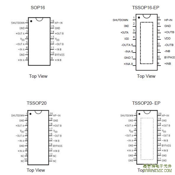
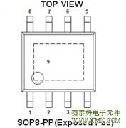
8.)The available in a SOP16 package and TSSOP16-P,TSSOP20 and TSSOP20-EP packages
三,应用范围 (Applications)
Multimedia monitors
Portable and desktop computers
Portable televisions
四.下载产品资料PDF文档
 |
JTM4863 |
六.电路原理图
七,功能概述
The exposed-DAP must be connected to ground.The exposed-DAP package of the JTM4863 re-
quires special attention to thermal design. If thermal design issues are not properly addressed,
an JTM4863 driving 4Ω will go into thermal shut-down.The exposed-DAP on the bottom of the JTM4863
should be soldered down to a copper pad on the circuit board. Heat is conducted away from the
exposed-DAP by a copper plane. If the copper plane is not on the top surface of the circuit board,
8 to 10 vias of 0.013 inches or smaller in diameter should be used to thermally couple the exposed-
DAP to the plane. For good thermal conduction,the vias must be plated-through and solder-filled.
The copper plane used to conduct heat away from the exposed-DAP should be as large as pratical. If
the plane is on the same side of the circuit board 2 operation into 4Ω. If the heat sink plane is buried
or not on the same side as the exposed-DAP, 5in 2 is the minimum for 5V operation into 4Ω. If the
ambient temperature is higher than 25°C, a larger copper plane or forced-air cooling will be required
to keep the JTM4863 junction temperature below the thermal shutdown temperature (150°C). See
the power derating curve for the JTM4863 for derating information.
The JTM4863 requires forced-air cooling when operating into 3Ω. With the part attached to 2.5in 2
of exposed copper,with a 3Ω load, and with an ambient temperature of 25°C,450 linear-feet per
minute kept the part out of thermal shutdown.In higher ambient temperatures, higher airflow
rates and/or larger copper areas will be required to keep the part out of thermal shutdown.
3Ω & 4 Ω L ay o u t C o n s i d er at i o n s With low impedance loads, the output power at
the loads is heavily dependent on trace resistance from the output pins of the JTM4863. Traces from
the output of the JTM4863 to the load or load connectors should be as wide as practical.Any
resistance in the output traces will reduce the power delivered to the load. For example, with a
4Ω load and 0.1Ω of trace resistance in each output, output power at the load drops from 2.2W
to 2.0W. Output power is also dependent on supply regulation. To keep the supply voltage
from sagging under full output power conditions,the supply traces should be as wide as practical.
B r i d g e Co n f i g u r at i o n E x p l an at i o n
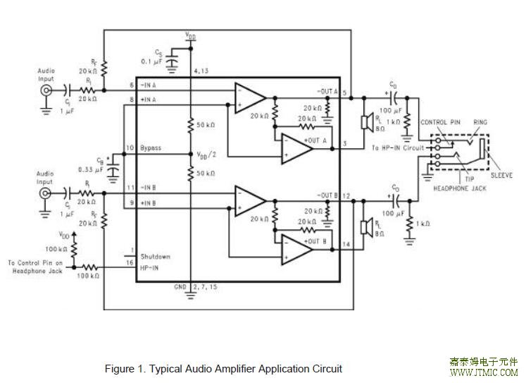
As shown in Figure 1, the JTM4863 has two pairs of operational amplifiers internally, allowing for
a few different amplifier configurations. Thefirst amplifier ’s gain is externally configurable,
while the second amplifier is internally fixed in a unity-gain, inverting configuration. The closed-
loop gain of the first amplifier is set by selecting the ratio of Rf to R i while the second amplifier ’s
gain is fixed by the two internal 20 kΩ resistors.Figure 1 shows that the output of amplifier one
serves as the input to amplifier two which resultsin both amplifiers producing signals identical in
magnitude, but out of phase180°.Consequently,the differential gain for eachchannel of the IC is
AVD = 2 * (R f/R i)
By driving the load differentially through outputs +OutA and −OutA or +OutB and −OutB, an
amplifier configuration commonly referred to as“bridged mode” is established. Bridged mode
operation is different from the classical single-ended amplifier configuration where one side of
its load is connected to ground.
八,相关产品
| AB类音频放大IC | ||||||||
| 型号 | 工作电 | 静态 | 输出 | 静态 | 纹波 | 通道 | 封装 | 代替型号 |
| 压范围 | 电流 | 功率 | 输出电压 | 抑制比 | 隔离度 | |||
| LM4871 | 2V-5.5V | 6.5mA | 2W/Vcc=5V | 5mV/Vcc=5V | 60dB | SOP8 | LM4871 | |
| Rl=3oJTM | ||||||||
| JTM8002 | 2V-5.5V | 6.5mA | 3W/Vcc=5V | 5mV/Vcc=5V | 60dB | SOP8 | CSC8002 | |
| Rl=3oJTM | ||||||||
| JTM4890 | 2.5V-5.5V | 4mA | 1W/Vcc=5V | 7mV/Vcc=5V | 62dB | MSOP8 | LM4890/LM4889/APA0711 | |
| Rl=8oJTM | /NCP2890/PT2366/BL6290 | |||||||
| /LPA4890 | ||||||||
| JTM4990 | 2.5V-5.5V | 2.5mA | 1.25W/Vcc=5V | 7mV/Vcc=5V | 62dB | MSOP-8 | LM4990/NCP2990 | |
| Rl=8oJTM | ||||||||
| JTM4863 | 2V-5.5V | 6mA | 2.5W/Vcc=5V | 50mV/Vcc=5V | 67dB | 90dB | TSSOP20-PP/ | LM4863/CSC4863 |
| Rl=3oJTM | SOP16/DIP16 | |||||||
| TDA2030A | 6V-22V | 50mA | 14W/Vcc=19V | 2mV | 54dB | TO220B-5L | TDA2030A/TDA2003 | |
| Rl=4oJTM | ||||||||
| TDA2822 | 1.8V--6V | 6mA | 0.35W/Vcc=3V | 1.2V/Vcc=3V | 30dB | 50dB | SOP8/DIP8 | TDA2822 |
| Rl=4oJTM | ||||||||
| TEA2025_9V | 3V--9V | 40mA | 2.3W/Vcc=9V | 4.5V/Vcc=9V | 46dB | 55dB | DIP16 | TEA2025 |
| Rl=4oJTM | ||||||||
| TEA2025_12V | 3V--12V | 40mA | 2.3W/Vcc=9V | 4.5V/Vcc=9V | 46dB | 55dB | DIP16 | TEA2025 |
| Rl=4oJTM | ||||||||
| D类音频放大IC | ||||||||
| 型号 | 工作电 | 静态 | 输出 | 静态 | 纹波 | 通道 | 封装 | 代替型号 |
| 压范围 | 电流 | 功率 | 输出电压 | 抑制比 | 隔离度 | |||
| JTM2010 | 2.4V-5.5V | 3.8mA | 3.0W/Vcc=5V | 1mV/Vcc=5V | 75dB | MSOP-8 | TPA2010/NCP2820/TS4962/ | |
| Rl=4oJTM | SOP-8 | EUA2010/A7013/LM4670/1/3/5 | ||||||
| APA2010/PT2333/PAM8303 | ||||||||
| EUP2036/TMPA2055 | ||||||||
| JTM145 | 2.7V-5.5V | 0.1uA | 3.2W/Vcc=5V | 10mV/Vcc=5V | 75dB | 85uV | MSOP8 | YDA145 |
| Rl=4oJTM | ||||||||
| JTM9305 | 2V-5.5V | 5W/Vcc=5V | ESOP8 | |||||
| Rl=2oJTM | ||||||||
| JTM8403 | 2V-5.5V | 16mA | 3.2W/Vcc=5V | 5mV/Vcc=6V | 58dB | 95dB | SOP16 | PAM8403 |
| Rl=4oJTM | ||||||||
| F类(AB类/D类可选)音频放大IC | ||||||||
| 型号 | 工作电 | 静态 | 输出 | 静态 | 纹波 | 通道 | 封装 | 代替型号 |
| 压范围 | 电流 | 功率 | 输出电压 | 抑制比 | 隔离度 | |||
| JTM8871 | 2V-5.5V | 5W/Vcc=5V | ESOP8 | |||||
| Rl=2oJTM | ||||||||
| 耳机音频放大IC | ||||||||
| 型号 | 工作电 | 静态 | 输出 | 静态 | 纹波 | 通道 | 封装 | 代替型号 |
| 压范围 | 电流 | 功率 | 输出电压 | 抑制比 | 隔离度 | |||
| JTM4800 | 2.7V-5.5V | 2.2mA | 0.29W/Vcc=5V | 5mV/Vcc=5V | 55dB | SOP-8 | TDA1308/LM4800/PT2308 | |
| Rl=8oJTM | APA4800/LM4808/G1402 | |||||||
| JTM4808 | 2.0V-5.5V | 1.2mA | 0.105W*2/Vcc=5V, | 10mV/Vcc=5V | 89dB | MSOP-8/ | ||
| Rl=16oJTM | SOP-8 | |||||||
| JTM4809 | 2.0V-5.5V | 1.4mA | 0.105W/Vcc=5V | 4mV/Vcc=5V | 70dB | MSOP-8 | LM4809/LM4880/HT82V735 | |
| Rl=16oJTM | APA4880 | |||||||
| JTM4811 | 2.0V-5.5V | 1.3mA | 0.105W/Vcc=5V | 4mV/Vcc=5V | 60dB | 100dB | MSOP10 | LM4811 |
| Rl=16oJTM | ||||||||
| 我司的JTM4871/SOP8/3W有如下优点: | ||||||||
| 1.工作电压2.0-5.5V,耐压6V | ||||||||
| 2.输出功率可以达3W/3OJTM和2.5W/4OJTM | ||||||||
| 3.没有交越失真的问题 | ||||||||
| 4.音质比较好,音量比较大,音质/音量可以和CSC8002媲美。 | ||||||||
| 我司的JTM8403/SOP16有如下优点: | ||||||||
| 1.工作电压范围在2.5-5.5V,耐压6V | ||||||||
| 2.输出功率可达3W/4 OJTM. | ||||||||
| 3.音量比较大,音质比较好,音质/音量可以和原装的PAM8403媲美。 | ||||||||
| 我司的JTM4863/SOP16&DIP16&TSSOP20有如下优点: | ||||||||
| 1.工作电压范围在2.0-5.5V,耐压6V | ||||||||
| 2.输出功率可达2.5W/3 OJTM-2.2W/4 OJTM. | ||||||||
| 3.音量比较大,音质比较好,音质/音量可以和CSC4863媲美。 | ||||||||
 JTM4103是一款降压恒流型
人气:255
JTM4103是一款降压恒流型
人气:255
 JTM6286,JTM6285 采用 60V 高压
人气:213
JTM6286,JTM6285 采用 60V 高压
人气:213
 The JTM6297,JTM6298,JTM6299 reg
人气:210
The JTM6297,JTM6298,JTM6299 reg
人气:210
 外驱MOSOS管,PSR控制模式,
人气:208
外驱MOSOS管,PSR控制模式,
人气:208
 The JTM1542 is a compact, high
人气:207
The JTM1542 is a compact, high
人气:207
 户外LED照明解决方案,通过
人气:204
户外LED照明解决方案,通过
人气:204
 JTM9921 是一款高效率,稳
人气:201
JTM9921 是一款高效率,稳
人气:201
 The JTM3106 is a 380 KHz fixed
人气:197
The JTM3106 is a 380 KHz fixed
人气:197
 The JTM1483,JTM1483A is a synch
人气:190
The JTM1483,JTM1483A is a synch
人气:190
 The JTM3501 is a 150 KHz fixed
人气:190
The JTM3501 is a 150 KHz fixed
人气:190
 粤ICP备13004986号-3