


目录
一,产品概述(General Description)
OVERLOAD RECOVERY
Overload recovery refers to regulator’s ability to recover from a short circuited output. A key factor in the recovery
process is the current limiting used to protect the output from drawing too much power. The current limiting circuit
reduces the output current as the input to output differential increases. Refer to short circuit curve in the curve section.
During normal start-up, the input to output differential is small since the output follows the input. But, if the output is
shorted, then the recovery involves a large input to output differential. Sometimes during this condition the current limiting
circuit is slow in recovering. If the limited current is too low to develop a voltage at the output, the voltage will stabilize at
a lower level. Under these conditions it may be necessary to recycle the power of the regulator in order to get the smaller
differential voltage and thus adequate start up conditions. Refer to curve section for the short circuit current vs. input
differential voltage.
THERMAL CONSIDERATIONS
ICs heats up when in operation, and power consumption is one factor in how hot it gets. The other factor is how well the
heat is dissipated. Heat dissipation is predictable by knowing the thermal resistance between the IC and ambient (θJA).
Thermal resistance has units of temperature per power (C/ W). The higher the thermal resistance, the hotter the IC.
The JTM1084 specifies the thermal resistance for each package as junction to case (θJC). In order to get the total
resistance to ambient (θJA), two other thermal resistances must be added, one for case to heat-sink (θCH) and one for
heatsink to ambient (θHA). The junction temperature can be predicted as follows:
TJ is junction temperature, TA is ambient temperature, and PD is the power consumption of the device. Device power
consumption is calculated as follows:
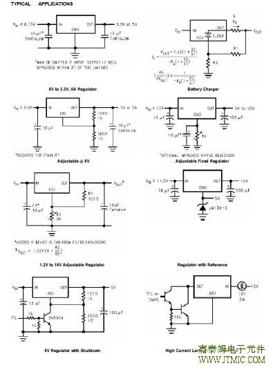
Figure 6 shows the voltages and currents which are present in the circuit.
二.产品特点(Features)
1.)Output Current : 5A
2.)Maximum Input Voltage : 12V
3.)Adjustable Output Voltage or Fixed 1.8V, 3.3V, 5.0V
4.)Current Limiting and Thermal Protection
5.)Standard 3-Pin Power Packages
三,应用范围 (Applications)
Post Regulator for Switching DC/DC Converter
High Efficiency Liner Regulators
Battery Charger
四.下载产品资料PDF文档
 |
JTM1084 |
六.电路原理图
七,功能概述
STABILITY CONSIDERATION
Stability consideration primarily concern the phase response of the feedback loop. In order for stable operation, the loop
must maintain negative feedback. The JTM1084 requires a certain amount series resistance with capacitive loads. This
series resistance introduces a zero within the loop to increase phase margin and thus increase stability. The equivalent
series resistance (ESR) of solid tantalum or aluminum electrolytic capacitors is used to provide the appropriate zero
(approximately 500 kHz).
The Aluminum electrolytic are less expensive than tantalums, but their ESR varies exponentially at cold temperatures;
therefore requiring close examination when choosing the desired transient response over temperature. Tantalums are a
convenient choice because their ESR varies less than 2:1 over temperature.
The recommended load/decoupling capacitance is a 10uF tantalum or a 50uF aluminum. These values will assure
stability for the majority of applications.
The adjustable versions allows an additional capacitor to be used at the ADJ pin to increase ripple rejection. If this is
done the output capacitor should be increased to 22uF for tantalums or to 150uF for aluminum.
Capacitors other than tantalum or aluminum can be used at the adjust pin and the input pin. A 10uF capacitor is a
reasonable value at the input. See Ripple Rejection section regarding the value for the adjust pin capacitor.
It is desirable to have large output capacitance for applications that entail large changes in load current (microprocessors
for example). The higher the capacitance, the larger the available charge per demand. It is also desirable to provide low
ESR to reduce the change in output voltage:
It is common practice to use several tantalum and ceramic capacitors in parallel to reduce this change in the output
voltage by reducing the overall ESR.
Output capacitance can be increased indefinitely to improve transient response and stability.
RIPPLE REJECTION
Ripple rejection is a function of the open loop gain within the feed-back loop (refer to Figure 1 and Figure 2). The JTM1084
exhibits 75dB of ripple rejection (typ.). When adjusted for voltages higher than VREF, the ripple rejection decreases as
function of adjustment gain: (1+R1/R2) or VO/VREF. Therefore a 5V adjustment decreases ripple rejection by a factor of
four (−12dB); Output ripple increases as adjustment voltage increases.
However, the adjustable version allows this degradation of ripple rejection to be compensated. The adjust terminal can
be bypassed to ground with a capacitor (CADJ). The impedance of the CADJ should be equal to or less than R1 at the
desired ripple frequency. This bypass capacitor prevents ripple from being amplified as the output voltage is increased.
LOAD REGULATION
The JTM1084 regulates the voltage that appears between its output and ground pins, or between its output and adjust pins.In some cases, line resistances can introduce errors to the voltage across the load. To obtain the best load regulation, a few precautions are needed.
Figure 3 shows a typical application using a fixed output regulator. Rt1 and Rt2 are the line resistances. VLOAD is less
than the VOUT by the sum of the voltage drops along the line resistances. In this case, the load regulation seen at the
RLOAD would be degraded from the data sheet specification. To improve this, the load should be tied directly to the output terminal on the positive side and directly tied to the ground terminal on the negative side.
八,相关产品
| 耐高压 LDO IC | ||||||||||
| 型号 | 最大输 | 输入电压 | 输出电压 | 精度 | 功耗 | 纹波 | 负载 | 线性 | 封装 | 替代型号 |
| 出电流 | (1KHZ) | 稳定率 | 稳定率 | |||||||
| JTM75XX | 150mA | 18V | 2.8/3.0/3.3/ | ±3% | 2uA | 50dB | 60mV | 0.20% | SOT-89/SOT-23 | HT75XX/HT71XX |
| 3.6/4.0/4.4/5.0V | TO-92 | HT10XX | ||||||||
| JTM75XXH | 150mA | 24V | 3.0/3.3/3.6/4.0/5.0V | ±2% | 2uA | 50dB | 60mV | 0.20% | SOT-89 | HT75XX/HT71XX |
| HT10XX | ||||||||||
| JTM75XXHB | 100mA | 40V | 3.3/5.0V | ±3% | 2.5uA | 60mV | 0.20% | SOT-89/TO-92 | HT75XX/HT71XX | |
| HT71XX | ||||||||||
| JTM73XX | 300mA | 18V | 1.5/1.8/2.5/2.7/2.8/3.0 | ±3% | 2uA | 50dB | 45mV | 0.20% | SOT-89/SOT-23-3L | HT73XX/HT75XX |
| 3.3/3.6/4.0/4.4/5.0V | TO-92 | HT71XX | ||||||||
| JTM73XXH | 300mA | 24V | 3.0/3.3/5.0V | ±2% | 2uA | 50dB | 45mV | 0.20% | SOT-89 | HT73XX/HT75XX |
| HT71XX | ||||||||||
| JTM78XX | 500mA | 18V | 1.8/2.5/2.7/2.8/3.0/ | ±2% | 1 uA | 12mV | 0.05% | SOT-89/SOT-23-3L | HT78XX | |
| 3.3/3.6/5.0V | ||||||||||
| HX53XX | 500mA | 12V | 1.2/1.5/1.8/2.1/2.5/ | ±2% | 1.2uA | 30mA | 0.05% | SOT-89/SOT23-3L | HT78XX | |
| 2.7/2.8/3.0/3.3/3.6/ | TO-92 | |||||||||
| 3.9/4.4/5.0V | ||||||||||
| JTM53XXB | 250mA | 40V | 3.0/3.3/3.6/5.0V | ±2% | 1.6uA | 20mV | 0.20% | SOT-89/SOT-23/ | ||
| TO-92 | ||||||||||
| JTM6203 | 100mA | 40V | 3.0/3.3/3.6/5.0V | ±2% | 3 uA | 30mV | 0.04% | SOT-89/SOT-23-3L | ||
| TO-92 | ||||||||||
| JTM6312 | 100mA | 40V | 3.0/3/3/5.0V | ±3% | 2.5uA | 60mA | 0.20% | SOT-89 | ||
| 大电流耐高压LDO IC | ||||||||||
| 型号 | 最大输 | 输入电压 | 输出电压 | 精度 | 功耗 | 纹波 | 负载 | 线性 | 封装 | 替代型号 |
| 出电流 | (1KHZ) | 稳定率 | 稳定率 | |||||||
| AMS1117 | 1A | 18V | 1.2/1.5/1.8/2.5/3.3/5.0V/可调 | ±1% | 4mA | 75dB | 3mV | - | SOT-223 | AMS1117 |
| TO-252 | LM1117 | |||||||||
| SOT89 | ||||||||||
| JTM1084 | 5A | 12V | 3.3/5.0V/可调 | ±1% | 5mA | 60dB | 15mV | - | TO-252 | AMS1084 |
| LM1084 | ||||||||||
| 带使能耐高压LDO IC | ||||||||||
| 型号 | 最大输 | 输入电压 | 输出电压 | 精度 | 功耗 | 纹波 | 负载 | 线性 | 封装 | 替代型号 |
| 出电流 | (1KHZ) | 稳定率 | 稳定率 | |||||||
| JTM53XX | 500mA | 12V | 1.8/2.5/2.8/3.0/3.3/3.6V/5.0V | ±2% | 1.2uA | 30mV | 0.05% | SOT-25 | ||
| JTM6209 | 400mA | 18V | 3.0/3.3/3.6/4.0/5.0V | ±2% | 60uA | 30mV | 0.03% | SOT-25 | ||
| JTM6221 | 350mA | 18V | 3.0/3.3/5.0V | ±2% | 8uA | 12mV | 0.05% | SOT-25 | ||
| 我司的JTM75XX/JTM73XX有以下优点: | ||||||||||
| 1.耐压可达18V | ||||||||||
| 2.静态电流小,只有2uA(典型值) | ||||||||||
| 3.有SOT-89/SOT-23/TO-92封装. | ||||||||||
| 4.封装采用金线,全测产品,一致性好,品质稳定. | ||||||||||
| 我司的AMS1117有如下优点: | ||||||||||
| 1.最大可达1A驱动电流 | ||||||||||
| 2.耐压可达18V. | ||||||||||
| 3.和市场低端的那种只有600-800mA/耐压只有9-12V的不同的。 | ||||||||||
| 4.封装种类齐全,有SOT-223/TO-252/SOT-89封装。 | ||||||||||
| 产品应用: | ||||||||||
| 1.小家电、家电控制板 | ||||||||||
| 2.电子秤、人体秤 | ||||||||||
| 3.电子玩具、电动玩具、遥控玩具 | ||||||||||
| 4.三表(电表、水表、煤气表) | ||||||||||
| 5.LED手电筒、LED照明产品 | ||||||||||
| 6.汽车防盗器、电子锁 | ||||||||||
 JTM4103是一款降压恒流型
人气:255
JTM4103是一款降压恒流型
人气:255
 JTM6286,JTM6285 采用 60V 高压
人气:213
JTM6286,JTM6285 采用 60V 高压
人气:213
 The JTM6297,JTM6298,JTM6299 reg
人气:210
The JTM6297,JTM6298,JTM6299 reg
人气:210
 外驱MOSOS管,PSR控制模式,
人气:208
外驱MOSOS管,PSR控制模式,
人气:208
 The JTM1542 is a compact, high
人气:207
The JTM1542 is a compact, high
人气:207
 户外LED照明解决方案,通过
人气:204
户外LED照明解决方案,通过
人气:204
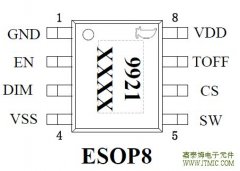 JTM9921 是一款高效率,稳
人气:201
JTM9921 是一款高效率,稳
人气:201
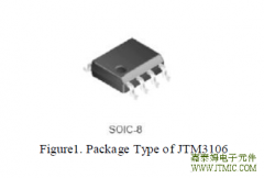 The JTM3106 is a 380 KHz fixed
人气:197
The JTM3106 is a 380 KHz fixed
人气:197
 The JTM1483,JTM1483A is a synch
人气:190
The JTM1483,JTM1483A is a synch
人气:190
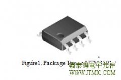 The JTM3501 is a 150 KHz fixed
人气:190
The JTM3501 is a 150 KHz fixed
人气:190
 粤ICP备13004986号-3