


目录
一,产品概述(General Description)
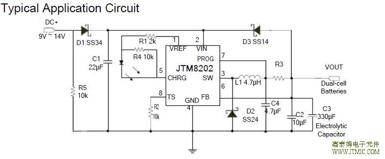
The JTM8202 is a complete battery charger controller for two (8.4V) cells lithium-ion batteries.The JTM8202 provides a small, simple and efficient
solution to fast charge Li-ion battery. An external sense resistor sets the charge current with high accuracy.
An internal resistor divider and precision reference set the final float voltage to 8.4V. When the input supply is removed, the JTM8202 automatically enters a low current sleep mode.
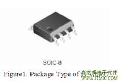
The JTM8202 is available in the SOP-8L package.
二.产品特点(Features)
1.)Input Supply Range: 9V ~ 14V
2.)End-Charge-Current Detection Output
3.)Constant Switching Frequency for Minimum Noise
4.)Automatic Battery Recharge
5.)Automatic Shutdown When Input Supply is Removed
6.)Automatic Trickle Charging of Low Voltage Batteries
7.)Battery Temperature Sensing
8.)Stable with Ceramic Output Capacitor
9.)SOP-8L Package
三,应用范围 (Applications)
Charging Docks
Handheld Instruments
Portable Computers
四.下载产品资料PDF文档
 |
jtm8202 |
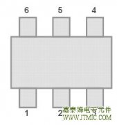
五,产品封装图 (Package)
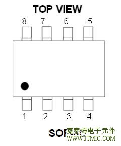
| PIN | NAME | FUNCTION |
| 1 | VREF | Voltage Reference to Drive LED |
| 2 | VIN | Input |
| 3 | SW | Switch Output |
| 4 | GND | Ground |
| 5 | CHRG | Open-Drain Charge Status for Output |
| 6 | FB | Feedback |
| 7 | PROG | Charge Current Program |
| 8 | TS | Temperature Sense |
六.电路原理图
七,功能概述
Current Regulation Phase
The JTM8202 regulates current while the battery-pack voltage is less than the regulation voltage, VO(REG).
The JTM8202 monitors charge current by the voltage drop across a sense-resistor, R3, in series with the
battery pack, and the resistor, R3, connected to the PROG pin. In order to set the current, first choose
R3 based on the regulation threshold VIREG = VPROG – VFB across this resistor. The following formula
calculates the value of the Sense resistor:
Battery Voltage Regulation
The voltage regulation feedback occurs through the FB pin. This input is tied to the positive side of the
battery pack. The JTM8202 monitors the battery-pack voltage between the FB and GND pins. The
JTM8202 is offered in a fixed two-cell voltage version (8.4 V).
Charge Termination Recharge
The JTM8202 monitors the charging current during the voltage-regulation phase. The JTM8202 declares a
done condition and terminates charge when the current drops to the charge termination threshold, ITERM.
A new charge cycle begins when the battery voltage falls below the VRCH threshold.
Battery Temperature Monitoring
A negative temperature coefficient (NTC) thermistor located close to the battery pack can be used to
monitor battery temperature and will not allow charging unless the battery temperature is within an
acceptable range.
Connect a 10kΩ thermistor from the TS pin to ground. With the 99.5µA pull-up current source, the hot
temperature voltage threshold is 479mV. For Cold temperature, the voltage threshold is set at 2.422V
with 99.5µA of pull-up current. The charge cycle begins or resumes once the temperature is within the
acceptable range.
Charge Status Indication
The JTM8202 reports the status of the charge on the CHRG pin. The following table summarized the
operation of the CHRG pin.
The CHRG pin can be used to drive a chip LED.
Low-Power Sleep Mode
When the input supply is disconnected, the charger automatically enters power-saving sleep mode. This
feature prevents draining the battery pack during the absence of VIN.
Input and Output Capacitors
Since the input capacitor is assumed to absorb all input switching ripple current in the converter, it must
have an adequate ripple current rating. Worst-case RMS ripple current is approximately one-half of
output charge current. Actual capacitance value is not critical. Solid tantalum capacitors have a high
ripple current rating in a relatively small surface mount package, but caution must be used when
tantalum capacitors are used for input bypass. High input surge currents can be created when the
adapter is hot-plugged to the charger and solid tantalum capacitors have a known failure mechanism
when subjected to very high turn-on surge currents. Selecting the highest possible voltage rating on the
capacitor will minimize problems. Consult with the manufacturer before use.
The selection of output capacitor COUT is primarily determined by ESR required to improve ripple voltage
and load transient. The output ripple ΔVOUT is approximately bounded by:
八,相关产品
| 2节锂电充电IC | |||||||||
| 型号 | 电池数量 | 工作模式 | 工作电压 | 最大 | 工作电流 | 恒流恒压 | 输出电压 | 开关频率 | 封装 |
| 充电电流 | 精度 | ||||||||
| JTM8203 | 两节 | 线性,内置MOS | 9V-16V | 1A | 0.26mA | 1% | 8.4V | SOP-8L | |
| JTM8202 | 两节 | 开关式,内置MOS | 9V-16V | 2A | 0.26mA | 1% | 8.4V | 780KHz | SOP-8L |
| JTM8207 | 两节 | 开关式,外置MOS | 8.9V-20V | 2A | 3.5mA | 1% | 8.4V | 500KHz | SOP-8L |
| JTM4060 | 单节/两节 | 开关式,外置MOS | 最大20V | 3A | 1% | 4.2V/CELL | 600KHz | MSOP-10 | |
| JTM4061 | 单节/两节 | 开关式,外置MOS | 4.5V-12V | 2A | 5mA | 1% | 4.175V/CELL | 400KHz | TSSOP-14 |
| JTM4062 | 两节 | 开关式,外置MOS | 7.5V-28V | 5A | 1.55mA | 1% | 8.4V | 300KHz | TSSOP-16 |
| 多节锂电充电IC | |||||||||
| 型号 | 电池数量 | 工作模式 | 工作电压 | 最大 | 工作电流 | 恒流恒压 | 输出电压 | 开关频率 | 封装 |
| 充电电流 | 精度 | ||||||||
| JTM4063 | 三节 | 开关式,外置MOS | 7.5V-28V | 5A | 1.75mA | 1% | 12.6V | 300KHz | TSSOP-16 |
| JTM4064 | 四节 | 开关式,外置MOS | 7.5V-28V | 5A | 1.95mA | 1% | 16.8V | 300KHz | TSSOP-16 |
| JTM4065 | 1-6节可设置 | 开关式,外置MOS | 7.5V-28V | 5A | 1.7mA | 1% | 可调 | 300KHz | TSSOP-16 |
| 型号 | 输入电压 | 最大充电电流 | 充电类型 | 单节截止电压 | 封装形式 | ||||
| JTM4058 | 2.6-7.5V | 250mA | 1到8节镍镉/镍氢电池充电IC | 1.35V | SOP-8 | ||||
| JTM4059 | 2.3-6.5V | 1.2A | 1到3节镍镉/镍氢/镍锌电池充电IC | 1.35V | ESOP8 | ||||
| JTM4059B | 3.1-6.5V | 1A | 1到4节镍镉/镍氢电池充电IC | 1.35V | ESOP8 | ||||
| JTM4068 | 7.5-28V | 扩流5A | 2-17节镍氢电池充电IC | 1.35V | TSSOP16 | ||||
| JTM4067 | 7.5-28V | 扩流5A | 单节/多节铅酸电池充电IC | 3.6V | TSSOP16 | ||||
| 型号 | 输入耐压 | 检测电压范围 | 检测电 | 输出形式 | 工作电流 | 封装 | 直接替代型号 | ||
| 压精度 | |||||||||
| JTM61C/NXX2 | 12V | 1.1/1.8/2.0/2.1/2.2/2.4/2.5/ | 2% | CMOS/N沟道 | 1.1uA | SOT-23 | XC61FC(N)/XC61CC(N)/ | ||
| 2.7/2.8/3.0/3.3/3.5/3.6/ | RT9808/RT9809/AIC1680/ | ||||||||
| 3.9/4.0/4.2/4.4/5.0V | AP8822/S808/UT81XX | ||||||||
| JTM70XX | 12V | 1.1/1.8/2.0/2.1/2.2/2.4/2.5/ | 2% | CMOS/N沟道 | 1.1uA | SOT-23 | HT70XX/KIA70XX | ||
| 2.7/2.8/3.0/3.3/3.5/3.6/ | SOT-89 | ||||||||
| 3.9/4.0/4.2/4.4/5.0V | TO-92 | ||||||||
| JTM6100 | 6.5V | 1.2V以上,可以设置 | 2% | CMOS | 1.8uA | SOT-25 | |||
| JTM809系列 | 6V | 2.63V/2.93V/3.08V/ | 1% | CMOS | 1.0uA | SOT-23 | MAX809/ | ||
| 4.00V/4.38V/4.63V | IMP809/AME8500 | ||||||||
| JTM810系列 | 6V | 2.63V/2.93V/3.08V/ | 2% | CMOS | 8.0uA | SOT-23 | MAX810/IMP810 | ||
| 4.38V/4.63V | |||||||||
| JTM811系列 | 6V | 2.93V/4.00V/ | 2% | CMOS | 8.0uA | SOT-143 | MAX811/IMP811 | ||
| 4.38V/4.63V | |||||||||
| 我司的JTM61C/NXXXMR/SOT-23有如下优点: | |||||||||
| 1.耐压可达12V | |||||||||
| 2.静态电流小,只有1uA(典型值). | |||||||||
| 3.输出方式有N沟道和CMOS 2种. | |||||||||
| 4.输出检测电压值范围广,从1.1V~5.0V可以定义各电压值, | |||||||||
| 可以每隔0.1V定制. | |||||||||
| 5.目前检测电压有1.1/1.8/2.0/2.2/2.4/2.5/2.7/2.8/3.0/3.3/3.5/3.6/3.9/4.0/4.2/4.4V | |||||||||
| 6.封装采用金线,全测产品,一致性好,品质稳定. | |||||||||
| 我司的JTM70XXMR/PR SOT-23/SOT-89有如下优点: | |||||||||
| 1.耐压可达12V | |||||||||
| 2.静态电流小,只有1uA(典型值). | |||||||||
| 3.输出方式是N沟道输出. | |||||||||
| 4.输出检测电压值范围广,从1.1V~5.0V可以定义各电压值, | |||||||||
| 可以每隔0.1V定制. | |||||||||
| 5.目前检测电压有1.1/1.8/2.0/2.2/2.4/2.5/2.7/2.8/3.0/3.3/3.5/3.6/3.9/4.0/4.2/4.4V | |||||||||
| 6.封装采用金线,全测产品,一致性好,品质稳定. | |||||||||
 JTM4103是一款降压恒流型
人气:255
JTM4103是一款降压恒流型
人气:255
 JTM6286,JTM6285 采用 60V 高压
人气:213
JTM6286,JTM6285 采用 60V 高压
人气:213
 The JTM6297,JTM6298,JTM6299 reg
人气:210
The JTM6297,JTM6298,JTM6299 reg
人气:210
 外驱MOSOS管,PSR控制模式,
人气:208
外驱MOSOS管,PSR控制模式,
人气:208
 The JTM1542 is a compact, high
人气:207
The JTM1542 is a compact, high
人气:207
 户外LED照明解决方案,通过
人气:204
户外LED照明解决方案,通过
人气:204
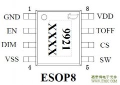 JTM9921 是一款高效率,稳
人气:201
JTM9921 是一款高效率,稳
人气:201
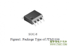 The JTM3106 is a 380 KHz fixed
人气:197
The JTM3106 is a 380 KHz fixed
人气:197
 The JTM1483,JTM1483A is a synch
人气:190
The JTM1483,JTM1483A is a synch
人气:190
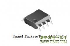 The JTM3501 is a 150 KHz fixed
人气:190
The JTM3501 is a 150 KHz fixed
人气:190
 粤ICP备13004986号-3