

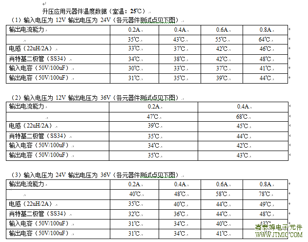
目录
一,产品概述(General Description)
The JTM6297 regulator is a wide input range,current mode, DC/DC converter which is capable of generating either positive or negative output voltages. It can be configured as either a boost, flyback, SEPIC or inverting converter. The JTM6297 built in N-
channel power MOSFET and fixed frequency oscillator, current-mode architecture results in stable operation over a wide range of supply
and output voltages.
The JTM6297 regulator is special design for portable electronic equipment.
二.产品特点(Features)
- Wide 3.6V to 24V Input Voltage Range
- Positive or Negative Output Voltage Programming with a Single Feedback Pin
- Current Mode Control Provides Excellent
- Transient Response 1.25V reference adjustable version
- Fixed 400KHz Switching Frequency
- Maximum 2A Switching Current
- SW PIN Built in Over Voltage Protection
- Excellent line and load regulation
- EN PIN TTL shutdown capability
- Internal Optimize Power MOSFET
- High efficiency up to 90%
- Built in Frequency Compensation
- Built in Soft-Start Function
- Built in Thermal Shutdown Function
- Built in Current Limit Function
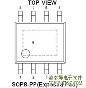
- Available in SOIC-8 package
-
Automotive and Industrial Boost/Buck-Boost / Inverting Convertersn
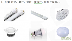
- Portable Electronic Equipment
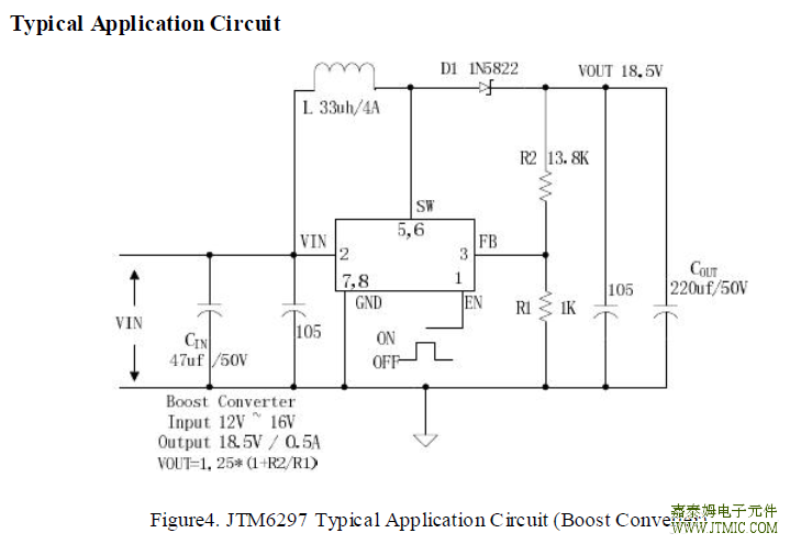
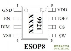
| Pin Number | Pin Name | Description |
| 1 | EN |
Enable Pin. Drive EN pin low to turn off the device, drive it high to turn it on. Floating is default high. |
| 2 | VIN |
Supply Voltage Input Pin. HM6297 operates from a 3.6V to 24V DC voltage. Bypass Vin to GND with a suitably large capacitor to eliminate noise on the input. |
| 3 | FB | Feedback Pin (FB). The feedback threshold voltage is 1.25V. |
| 4 | NC | No Connected. |
| 5,6 | SW |
Power Switch Output Pin (SW). Output is the switch node that supplies power to the output. |
| 7,8 | GND | Ground Pin. |
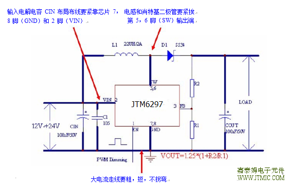
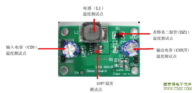
六, 产品PCB
PCB 板布局建议:
(1)流大电流的线要粗,短,不拐弯。
(2)7,8 脚(GND),2 脚(VIN)线要粗,短线,不拐弯,且输入电解电容 CIN 和 105 C1 陶瓷电容紧挨第 2 脚(VIN)和 7,8 脚(GND)。(主要是为
了减小输入电源布线寄生的电感,电阻产生的高压开关毛刺干扰)
(3)5,6 脚(SW)输出线要粗,短线,不拐弯,电感和续流二极管要紧挨第
5,6 脚(SW)输出端。
(4)3 脚(FB)走线要接到输出滤波电容 C2,COUT 之后, PCB 布线远离 L1,D1,
避免噪声干扰。
七.产品BOM
(略)
八.产品PDF文档
 |
JTM6297 |
十,相关产品
| 型号 | 工作模式 | 工作电压 | 输出 | 输出电压 | 输出电压 | 内置MOS | 效率 | 静态 | 工作频率 | 封装 |
| 范围 | 电压 | 形式 | 精度 | 最大输出 | 电流 | |||||
| 电流 | ||||||||||
| JTM6297 | PWM | 3.6V-26V | 最大60V | 可调输出 | ±2% | 2A | 90% | 70uA | 400KHz | SOP-8 |
| JTM6298 | PWM | 3.6V-36V | 最大60V | 可调输出 | ±2% | 3A | 92% | 70uA | 400KHz | TO252-5L |
| JTM6299 | PWM | 5V-45V | 最大60V | 可调输出 | ±2% | 5A | 94% | 70uA | 220KHz | TO263-5L |
 JTM4103是一款降压恒流型
人气:255
JTM4103是一款降压恒流型
人气:255
 JTM6286,JTM6285 采用 60V 高压
人气:213
JTM6286,JTM6285 采用 60V 高压
人气:213
 外驱MOSOS管,PSR控制模式,
人气:208
外驱MOSOS管,PSR控制模式,
人气:208
 The JTM1542 is a compact, high
人气:207
The JTM1542 is a compact, high
人气:207
 户外LED照明解决方案,通过
人气:204
户外LED照明解决方案,通过
人气:204
 JTM9921 是一款高效率,稳
人气:201
JTM9921 是一款高效率,稳
人气:201
 The JTM3106 is a 380 KHz fixed
人气:197
The JTM3106 is a 380 KHz fixed
人气:197
 The JTM1483,JTM1483A is a synch
人气:190
The JTM1483,JTM1483A is a synch
人气:190
 The JTM3501 is a 150 KHz fixed
人气:190
The JTM3501 is a 150 KHz fixed
人气:190
 粤ICP备13004986号-3