电路原理图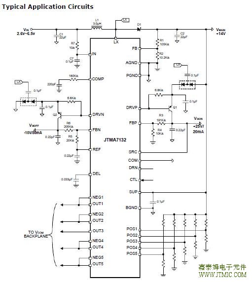 七,功能概述 For all switching power supplies, the layout is an impor-tant step in the design; especially at high peak currents and switching frequencies. There are some general guidelines for layout: 1.Place the external power components (the input capacitors, output capacitors, boost inductor and output diodes, etc.) in close proximity to the device.Traces to these components should be kept as short and wide as possible to minimize parasitic inductance and resistance. 2.Place the REF and IN bypass capacitors close to the pins. The ground connection of the IN bypass capacitor should be connected directly to the AGND pin with a wide trace. 3.Create a power ground (PGND) and a signal ground island and connect at only one point. The power ground consisting of the input and output capacitor grounds, PGND pin, and any charge-pump components. Connect all of these together with short, wide traces or a small ground plane. Maxi- mizing the width of the power ground traces im-proves efficiency and reduces output voltage ripple and noise spikes. The analog ground plane (AGND) consisting of the AGND pin, all the feed- back-divider ground connections, the operational-amplifier divider ground connections, the COMP and DEL capacitor ground connections, and the device’s exposed backside pad. Connect the AGND and PGND islands by connecting the PGND pin directly to the exposed backside pad. Make no other connections between these separate ground planes. 4.The feedback network should sense the output volt-age directly from the point of load, and be as far away from LX node as possible. 5.The exposed die plate, underneath the package,should be soldered to an equivalent area of metal on the PCB. This contact area should have mul-tiple via connections to the back of the PCB as well as connections to intermediate PCB layers, if available, to maximize thermal dissipation away from the IC. 6.To minimize the thermal resistance of the package when soldered to a multi-layer PCB, the amount of copper track and ground plane area connected to the exposed die plate should be maximized and spread out as far as possible from the IC. The bot-tom and top PCB areas especially should be maxi- mized to allow thermal dissipation to the surround-ing air. 7.Minimize feedback input track lengths to avoid switching noise pick-up 八,相关产品
(责任编辑:oumao18) |
|||||||||||||||||||||||||||||||||||||||||||||||||||||||||||||||||||||||||||||||||||||||||||||||||||||||||||||||||||||||||||||||||||||||

 粤ICP备13004986号-3