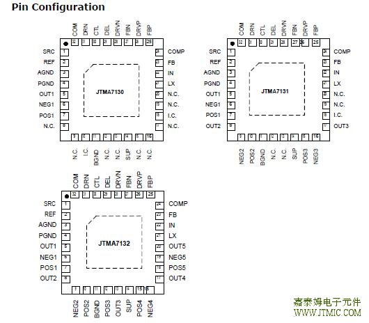
|
Pin |
Name |
Function Description |
|
JTMA7130 |
JTMA7131 |
JTMA7132 |
|
1 |
|
SRC |
SRC |
SRC |
Switch Input. Source of the internal high-voltage P-channel MOSFET. Bypass
SRC to PGND with a minimum of 0.1µF capacitor closed to the pins. |
|
2 |
REF |
REF |
REF |
Reference voltage output. Bypass REF to AGND with a minimum of
0.22µFcapacitor closed to the pins. |
|
3 |
AGND |
AGND |
AGND |
Analog Ground for Step-Up Regulator and Linear Regulators. Connect to
power ground (PGND) underneath the IC. |
|
4 |
PGND |
PGND |
PGND |
Power Ground for Step-Up Regulator. PGND is the source of the main step-up
n-channel power MOSFET. Connect PGND to the ground terminals of output
capacitors through a short, wide PC board trace. Connect to analog ground
(AGND) underneath the IC. |
|
5 |
OUT1 |
OUT1 |
OUT1 |
Output of Operational-Amplifier 1 |
|
6 |
NEG1 |
NEG1 |
NEG1 |
Inverting Input of Operational-Amplifier 1 |
|
7 |
POS1 |
POS1 |
POS1 |
Non-inverting Input of Operational-Amplifier 1 |
|
8 |
NC |
OUT2 |
OUT2 |
Output of Operational-Amplifier 2 of JTMA7132/JTMA7131. No internal
connected of JTMA7130. |
|
9 |
NC |
NEG2 |
NEG2 |
Inverting Input of Operational-Amplifier 2 of JTMA7132/JTMA7131. No internal
connected of JTMA7130. |
|
10 |
IC |
POS2 |
POS2 |
Non-inverting Input of Operational-Amplifier 2 of JTMA7132/JTMA7131. Internal
connected to GND of JTMA7130 |
|
11 |
BGND |
BGND |
BGND |
Analog Ground for Operational Amplifiers. Connect to power ground (PGND)
underneath the IC. |
|
12 |
NC |
NC |
POS3 |
Non-inverting Input of Operational-Amplifier 3 of JTMA7132. No internal
connected of JTMA7131/JTMA7130. |
|
13 |
NC |
NC |
OUT3 |
Output of Operational-Amplifier 3 of JTMA7132. No internal connected of
JTMA7131/JTMA7130. |
|
14 |
SUP |
SUP |
SUP |
Power Input of Operational Amplifiers. Typically connected to VMAIN. Bypass
SUP to BGND with a 0.1µF capacitor. |
|
15 |
NC |
POS3 |
POS4 |
Non-inverting Input of Operational-Amplifier 4 of JTMA7132. Non-inverting
Input of Operational-Amplifier 3 of JTMA7131. No internal connected of
JTMA7130. |
|
16 |
NC |
NEG3 |
NEG4 |
Inverting Input of Operational-Amplifier 4 of JTMA7132. Inverting Input of
Operational-Amplifier 3 of JTMA7131. No internal connected of JTMA7130. |
|
17 |
NC |
OUT3 |
OUT4 |
Output of Operational-Amplifier 4 of JTMA7132. Output of
Operational-Amplifier 3 of JTMA7131. No internal connected of JTMA7130. |
|
18 |
IC |
IC |
POS5 |
Non-inverting Input of Operational-Amplifier 5 of JTMA7132. Internal connected
to GND of JTMA7131/JTMA7130. |
|
19 |
NC |
NC |
NEG5 |
Inverting Input of Operational-Amplifier 5 of JTMA7132. No internal connected
of JTMA7131/JTMA7130. |
|
20 |
NC |
NC |
OUT5 |
Output of Operational-Amplifier 5 of JTMA7132. No internal connected of
JTMA7131/JTMA7130. |
|
21 |
LX |
LX |
LX |
N-Channel Power MOSFET Drain and Switching Node. Connect the inductor
and Schottky diode to LX and minimize the trace area for lowest EMI. |
|
22 |
IN |
IN |
IN |
Supply Voltage Input. Bypass IN to AGND with a 0.1µF capacitor. IN can range
from 2.6V to 6.5V. |
|
23 |
FB |
FB |
FB |
Step-Up Regulator Feedback Input. Connect a resistive voltage-divider from
the output (VMAIN) to FB to analog ground (AGND). Place the divider within
5mm of FB. |
|
24 |
COMP |
COMP |
COMP |
Step-Up Regulator Error-Amplifier Compensation Point. Connect a series RC
from COMP to AGND. |

 粤ICP备13004986号-3