

目录
一,产品概述(General Description)
The JTM1485 is a synchronous step down regulator with CC control from a high voltage input supply. Operating with an input voltage
range of 8V ~ 30V, the JTM1485 achieves 3.5A continuous output current with excellent load and line regulation. The switching frequency is programmable from 100KHz to 500KHz and the synchronous architecture
provides for highly efficient designs. Current mode operation provides fast transient response and eases loop stabilization.
The JTM1485 requires a minimum number of readily available standard external components. Other features include cable compensation programmable current limit and thermal shutdown.
range of 8V ~ 30V, the JTM1485 achieves 3.5A continuous output current with excellent load and line regulation. The switching frequency is programmable from 100KHz to 500KHz and the synchronous architecture
provides for highly efficient designs. Current mode operation provides fast transient response and eases loop stabilization.
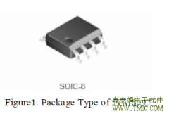
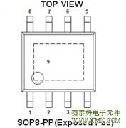
The JTM1485 converters are available in the industry standard SOP8-PP packages
二.产品特点(Features)
- Wide Input Voltage Range: 8V ~ 30V
- Up to 93% Efficiency
- Programmable Switching Frequency up
- to 500KHz
- No Loop Compensation Required
- CC/CV control
- Programmable CC Current
- Thermal Shutdown
- Available in SOP8-PP Package
-
Car Charger / Adaptor
-
LED Driver
-
Pre-Regulator for Linear Regulators
-
Distributed Power Systems
-
Battery ChargerCar Charger / Adaptor
-
LED Driver
-
Pre-Regulator for Linear Regulators
-
Distributed Power Systems
- Battery Charger

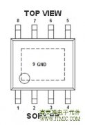
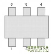
| PIN | NAME | DESCRIPTION |
| 1 | FB | Feedback |
| 2 | ILIM | CC Current Settng |
| 3 | EN | Enable |
| 4 | PDRI | PMOS Gate Drive |
| 5 | NDRI | NMOS Gate Drive |
| 6 | VIN | Input Supply Voltage |
| 7 | RT | Frequency setting |
| 8 | SW | Switch Node |
| 9 | GND | Ground |
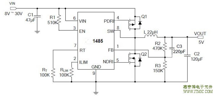
五,电路原理图
六, 产品PCB
(略)
七.产品BOM
(略)
八.产品PDF文档
 |
JTM1485 |
九,功能概述
Application Information
The JTM1485 operates by a constant frequency, current mode architecture. The output voltage is set
by an external divider returned to the FB pin. An error amplifier compares the divided output voltage with
a reference voltage of 1.21V and adjusts the peak inductor current accordingly.
Thermal Protection
The total power dissipation in JTM1485 is limited by a thermal protection circuit. When the device
temperature rises to approximately +160°C, this circuit turns off the output, allowing the IC to cool. The
thermal protection circuit can protect the device from being damaged by overheating in the event of fault
conditions. Continuously running the JTM1485 into thermal shutdown degrades device reliability.
Current Limit
Current limit detection occurs during the off-time by monitoring the current through the low-side switch
using an external resistor, RLIM. The current limit value is defined by RLIM. If during the off-time the
current in the low-side switch exceeds the user defined current limit value, the next on-time cycle is
immediately terminated. Current sensing is achieved by comparing the voltage across the low side FET
with the voltage across the current limit set resistor RLIM. For example, the current limit value is 4.5A by
the RLIM =100K. The current limit value rises when the set resistor RLIM rises. The maximum output
current is set by RLIM: RLIM (kΩ) = 1500 · IMAX (A) / RDS_PMOS (mΩ).
Oscillator Frequency
The JTM1485 oscillator frequency is set by a single external resistor connected between the RT pin and
the GND pin. The resistor should be located very close to the device and connected directly to the pins
of the IC (RT and GND). An internal amplifier holds the RT pin at a fixed voltage typically 0.6V. The
oscillator frequency rises when the resistor RT falls. To determine the timing resistance for a given
switching frequency, use the equation below:
RT(kΩ)= 22000 /fOSC(kHz)
Setting Output Voltage
The output voltage is set with a resistor divider from the output node to the FB pin. It is recommended to
use divider resistors with 1% tolerance or better. To improve efficiency at very light loads consider using
larger value resistors. If the values are too high the regulator is more susceptible to noise and voltage
errors from the FB input current are noticeable. For most applications, a resistor in the 10kΩ to 1MΩ
range is suggested for R3. R2 is then given by:
R2 = R3 · [(VOUT / VREF) – 1]
where VREF is 1.21V.
Output Cable Resistance Compensation
To compensate for resistive voltage drop across the charger's output cable, the JTM1485 integrates a
simple, user-programmable cable voltage drop compensation using the impedance at the FB pin.
Choose the proper feedback resistance values for cable compensation refer to the curve in Figure 1.
The delta VOUT voltage rises when the feedback resistance R3 value rises, use the equation below
十,相关产品
| 单P沟道低压MOS场效应管 | ||||||||||
| 型号 | 沟道 | VDS | VGS | VTH | ID | IDM | RDS(on) | 封装 | 状态 | 直接替代型号 |
| (Max) | (Max) | (Max) | ||||||||
| JTM2301/A | P沟道 | -20V | -10V | -0.7V | -3A | -10A | 65mΩ | SOT23 | 量产 | Si2301/AP2301/SI2305/XP152A/ |
| SOT23-3L | IRLML6401/IRML6402/AO3423 | |||||||||
| JTM2301B | P沟道 | -20V | -12V | -0.7V | -2.8A | -10A | 83mΩ | SOT23 | 量产 | Si2301/AP2301/XP152A/ |
| IRLML6402/AO3423 | ||||||||||
| JTM2301C | P沟道 | -12V | -12V | -0.7V | -2.8A | -10A | 85mΩ | SOT23 | 量产 | Si2301/AP2301/XP152A/ |
| IRLML6402/AO3423 | ||||||||||
| JTM2305 | P沟道 | -20V | -12V | -0.7V | -4.1A | -15A | 39mΩ | SOT23 | 量产 | Si2305/AP2305/APM2305/ |
| IRLML6401/IRML6402/AO3423 | ||||||||||
| JTM2333 | P沟道 | -12V | -12V | 0.32V | 6A | 20A | 30mΩ | SOT23-3L | 量产 | Si2333/IRLML6302 |
| JTM2341/B | P沟道 | -30V | -20V | -1V | -4.2A | -30A | 50mΩ | SOT23-3L | 量产 | WPM2341/Si2341/AO3401 |
| SOT23 | AO3415/IRLML6401/SI2307 | |||||||||
| JTM3401/B | P沟道 | -30V | -20V | -1V | -4.2A | -30A | 50mΩ | SOT23-3L | 量产 | AO3401/AO3415/IRLML6401 |
| SOT23 | /IRLML6402/SI2307 | |||||||||
| JTM3401C | P沟道 | -30V | -20V | -1.6V | -2.5A | -10A | 72mΩ | SOT23 | 量产 | AO3401/AO3407/AO3415/ |
| IRLML6401/IRLML6402/SI2307 | ||||||||||
| JTM3407/B | P沟道 | -30V | -20V | -1.5V | -4.2A | -20A | 55mΩ | SOT23-3L | 量产 | AO3407/AO3415/IRLML6401 |
| SOT23 | IRLML6402/SI2307 | |||||||||
| JTM3413/B | P沟道 | -20V | -12V | -0.7V | -2.5A | -10A | 118mΩ | SOT23-3L | 量产 | AO3413 |
| SOT23 | ||||||||||
| JTM3415E | P沟道 | -20V | -10V | -0.65V | -4.0A | -30A | 34mΩ | SOT23-3L | 量产 | AO3415 |
| 带ESD保护 | ||||||||||
| JTM3421/B | P沟道 | -30V | -20V | -1V | -4.2A | -30A | 50mΩ | SOT23-3L | 量产 | AO3421/AO3401/AO3415 |
| SOT23 | WPM2341/IRLML6401/SI2307 | |||||||||
| JTM2319 | P沟道 | -40V | -20V | -1.5V | -5.3A | -20A | 73mΩ | SOT-23-3L | 量产 | Si2319 |
| JTM2309 | P沟道 | -60V | -20V | -1.0V | -1.8A | -7A | 170mΩ | SOT-23-3L | 量产 | Si2309 |
| JTM6401 | P沟道 | -30V | -20V | -1V | -5.0A | -30A | 50mΩ | SOT23-6L | 量产 | AO6401/Si3481/APM2605/AO6405 |
| Si3455/SI3457/FDC634P/FDC636P | ||||||||||
| JTM9435 | P沟道 | -30V | -20V | -1.6V | -5.1A | -20A | 48mΩ | SOP8 | 量产 | CEM9435/APM9435/AP9435/ |
| Si9435/FDS9435/AO4405 | ||||||||||
| JTM9435B | P沟道 | -20V | -10V | -0.7V | -5A | -20A | 60mΩ | SOP8 | 量产 | CEM9435/APM9435/AP9435/ |
| Si9435/FDS9435/AO4405 | ||||||||||
| JTM4435 | P沟道 | -30V | -20V | -1.5V | -9.1A | -50A | 15mΩ | SOP8 | 量产 | AO4435/CEM4435/APM4435/ |
| AP4435/Si4435/FDS4435 | ||||||||||
| JTM4407 | P沟道 | -30V | -20V | -1.65V | -12A | -60A | 14mΩ | SOP8 | 量产 | AO4407/CEM4407/APM4407/ |
| AP4407/Si4407/FDS4407 | ||||||||||
| JTM4409 | P沟道 | -30V | -20V | -1.75V | -15A | -80A | 8mΩ | SOP8 | 量产 | AO4409/AO4407/AO4435/CEM4435 |
| APM4435/AP4435/Si4435/FDS4435 | ||||||||||
| JTM4443 | P沟道 | -40V | -20V | -1.5V | -6A | -24A | 73mΩ | SOP8 | 量产 | AO4443 |
| IRF7241 | ||||||||||
| JTM4485 | P沟道 | -40V | -20V | -2.0V | -15A | -60A | 30mΩ | SOP8 | 量产 | AO4485 |
| IRF7240 | ||||||||||
| JTM4441 | P沟道 | -55V | -20V | -2.6V | -5A | -25A | 64mΩ | SOP8 | 量产 | AO4441/AO4421/ |
| AO4443 | ||||||||||
| JTM5853 | P沟道+肖特基 | 22V | 8V | 0.69V | 3A | 12A | 110mΩ | DFN2*3-8 | 量产 | Si5853/AON4703/NHPD4P02 |
| JTM16P12D | P沟道 | 12V | 12V | 0.7V | 16A | 65A | 18mΩ | DNF2*2-6 | 量产 | AON2701/AON2401/3/5/IRLHS2242 |
 JTM4103是一款降压恒流型
人气:255
JTM4103是一款降压恒流型
人气:255
 JTM6286,JTM6285 采用 60V 高压
人气:213
JTM6286,JTM6285 采用 60V 高压
人气:213
 The JTM6297,JTM6298,JTM6299 reg
人气:210
The JTM6297,JTM6298,JTM6299 reg
人气:210
 外驱MOSOS管,PSR控制模式,
人气:208
外驱MOSOS管,PSR控制模式,
人气:208
 The JTM1542 is a compact, high
人气:207
The JTM1542 is a compact, high
人气:207
 户外LED照明解决方案,通过
人气:204
户外LED照明解决方案,通过
人气:204
 JTM9921 是一款高效率,稳
人气:201
JTM9921 是一款高效率,稳
人气:201
 The JTM3106 is a 380 KHz fixed
人气:197
The JTM3106 is a 380 KHz fixed
人气:197
 The JTM1483,JTM1483A is a synch
人气:190
The JTM1483,JTM1483A is a synch
人气:190
 The JTM3501 is a 150 KHz fixed
人气:190
The JTM3501 is a 150 KHz fixed
人气:190
 粤ICP备13004986号-3