


一,产品概述(General Description)
The JTM1583 is a 380KHz fixed frequency PWM buck (step-down) DC/DC converter, capable of driving a 3A load with high efficiency, low ripple and excellent line and load regulation. Requiring a minimum number of external components, the regulator is simple to use and include internal frequency compensation and a fixed-frequency oscillator
The PWM control circuit is able to adjust the duty ratio linearly from 0 to 100%. An enable function, an over current protection function is built inside. When short protection function happens, the operation frequency will be reduced from 380KHz to 80KHz. An internal compensation block is built in to minimize external component count
二.产品特点(Features)
- Wide 3.6V to 23V Input Voltage Range
- Output Adjustable from 1.222V to 21V
- Maximum Duty Cycle 100%
- Minimum Drop Out 0.6V
- Fixed 380KHz Switching Frequency
- 3A Constant Output Current Capability
- Internal Optimize Power MOSFET
- High efficiency
- Excellent line and load regulation
- TTL shutdown capability
- EN pin with hysteresis function
- Built in thermal shutdown function
- Built in current limit function
- Built in output short protection function
- Available in SOP8 package
LCD Monitor and LCD TV
Digital Photo FrameSet-up Box
ADSL Modem
Telecom / Networking Equipment
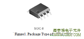
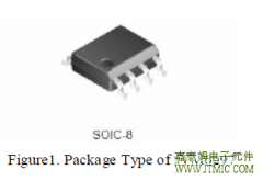
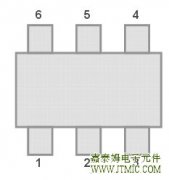
四,产品封装图 (Package)
| Pin Number | Pin Name | Description |
| 1,6,8 | NC | No Connected. |
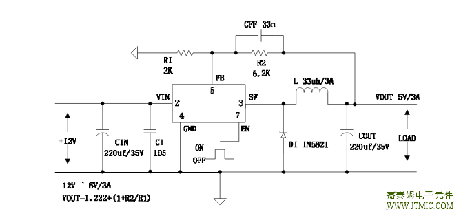
| 2 | VIN |
Supply Voltage Input Pin. JTM1583 operates from a 3.6V to 23V DC voltage. Bypass Vin to GND with a suitably large capacitor to eliminate noise on the input. |
| 3 | SW |
Power Switch Output Pin (SW). Output is the switch node that supplies power to the output. |
| 4 | GND |
Ground Pin. Care must be taken in layout. This pin should be placed outside of the Schottky Diode to output capacitor ground path to prevent switching current spikes from inducing voltage noise into JTM1583. |
| 5 | FB |
Feedback Pin (FB). Through an external resistor divider network, Feedback senses the output voltage and regulates it. The feedback threshold voltage is 1.222V. |
| 7 | EN |
Enable Pin. Drive EN pin low to turn off the device, drive it high to turn it on. Floating is default high. |
五,电路原理图
六, 产品PCB
(略)
七.产品BOM
Schottky Diode Selection Table
| Current |
Surface Mount |
Through Hole |
VR (The same as system maximum input voltage) | ||||
| 20V | 30V | 40V | 50V | 60V | |||
| 1A | √ | 1N5817 | 1N5818 | 1N5819 | |||
| 3A | √ | 1N5820 | 1N5821 | 1N5822 | |||
| √ | MBR320 | MBR330 | MBR340 | MBR350 | MBR360 | ||
| √ | SK32 | SK33 | SK34 | SK35 | SK36 | ||
| √ | 30WQ03 | 30WQ04 | 30WQ05 | ||||
| √ | 31DQ03 | 31DQ04 | 31DQ05 | ||||
| √ | SR302 | SR303 | SR304 | SR305 | SR306 | ||
八.产品PDF文档
 |
JTM1583 |
|
|
JTM1583A |
JTM1583 Electrical Characteristics
Ta = 25℃;unless otherwise specified.
| Symbol | Parameter | Test Condition | Min. | Typ. | Max. | Unit |
| System parameters test circuit figure4 | ||||||
| VFB |
Feedback Voltage |
Vin = 7V to 25V, Vout=5V Iload=0.2A to 3A |
1.186 | 1.222 | 1.258 | V |
| Efficiency | ŋ |
Vin=12V ,Vout=5V Iout=3A |
- | 89 | - | % |
Electrical Characteristics (DC Parameters)
Vin = 12V, GND=0V, Vin & GND parallel connect a 220uf/50V capacitor; Iout=500mA, Ta =
25℃; the others floating unless otherwise specified.
| Parameters | Symbol | Test Condition | Min. | Typ. | Max. | Unit |
| Input operation voltage | Vin | 3.6 | 23 | V | ||
| Shutdown Supply Current | ISTBY | VEN=0V | 60 | 200 | uA | |
| Quiescent Supply Current | Iq |
VEN =2V, VFB =Vin |
3 | 5 | mA | |
| Oscillator Frequency | Fosc | 323 | 380 | 437 | Khz | |
| Switch Current Limit | IL | VFB =0 | 4.7 | A | ||
| EN Pin Threshold | VEN |
High (Regulator ON) Low (Regulator OFF) |
1.4 0.8 |
V | ||
|
EN Pin Input Leakage Current |
IH | VEN =2V (ON) | 1 | 15 | uA | |
| IL | VEN =0V (OFF) | 1 | 15 | uA | ||
| Max. Duty Cycle | DMAX | VFB=0V | 100 | % |
Absolute Maximum Ratings (Note 1)
VIN Pin Voltage……………………………………………………………………….………-0.3V ~ 20V
SW Pin Voltage………………………………………………………………………-0.3V ~ (VIN + 0.3)V
FB Pin Voltage……………………………………………………………………………….....-0.3V ~ 6V
Operating Temperature Range(Note 2) ………………………………………………...-40℃ ~ + 85℃
Storage Temperature Range ……………………………………………….………….-65℃ ~ + 150℃
Junction Temperature Range…………………………………………………..………-40℃ ~ +125℃
Lead Temperature (Soldering 10, sec.) …………………………………………………………..+ 265℃
Note 1: Stresses listed as the above “Absolute Maximum Ratings” may cause permanent damage to the device.
Exposure to absolute maximum rating conditions for extended periods may remain possibility to affect device reliability.
Note 2: The JTM1583A is guaranteed to meet performance specifications from 0°C to 70°C. Specifications over the –40°C
to 85°C operating temperature range are assured by design, characterization and correlation with statistical process
controls.
十,相关产品
| DC-DC降压IC | ||||||||||
| 型号 | 输入耐压 | 输出电压 | 输出电流 | 反馈电压 | 工作频率 | 效率 | 静态 | 待机电流 | 封装 | 直接替换 |
| 工作电流 | ||||||||||
| LM2596 | 45V | 5.0V/可调输出 | 3A | 1.23V | 150K | 90% | 10mA | 80uA | TO-263-5L | LM2596/AP1501 |
| /3.3/12V | (Max) | TO-220-5L | ||||||||
| LM2576 | 45V | 5.0V/可调输出 | 3A | 1.23V | 50K | 90% | 10mA | 80uA | TO-263-5L | LM2576 |
| /3.3/12V | (Max) | TO-220-5L | ||||||||
| JTM1507 | 45V | 5.0V/可调输出 | 3A | 1.23V | 380K | 73% | 2mA | 0.2uA | TO-252-5L | AP1507 |
| MP1410 | 27V | 可调输出 | 2A | 1.22V | 420K | 95% | 1mA | 25uA | SOP8 | MP1410/ACT4060 |
| MP9141/RT826 | ||||||||||
| AP1534 | ||||||||||
| JTM1509 | 45V | 5.0V/可调输出 | 2A | 1.23V | 150K | 82% | 2mA | 80uA | SOP8 | AP1509 |
| 3.3V/12V | ||||||||||
| JTM1513 | 20V | 可调输出 | 2A | 0.8V | 150K | 89% | 2mA | 1uA | SOP-8 | AP1513 |
| JTM1530 | 20V | 可调输出 | 3A | 0.8V | 380K | 88% | 3mA | 1uA | SOP-8 | AP1510 |
| JTM1583 | 28V | 可调输出 | 3A | 1.22V | 380K | 89% | 3mA | 1uA | SOP-8 | MP1583 |
| JTM3111 | 42V | 可调输出 | 3A | 0.8V | 50-500K | 91% | 3mA | 150uA | ESOP8 | AX3111 |
| JTM3112 | 40V | 可调输出/ | 2A | 1.18V | 110K | 93% | 10mA | 2mA | SOP8 | |
| 带CC/CV模式 | ||||||||||
| JTM3113B | 40V | 可调输出/ | 2.5A | 1.0V | 250K | 91% | 10mA | 2mA | ESOP8 | |
| 带CC/CV模式 | ||||||||||
| JTM3101 | 45V | 可调输出/ | 2A | 1.235V | 150K | 83% | 2.0mA | ESOP8 | ||
| 带CC模式 | ||||||||||
| JTM3102 | 45V | 可调输出/ | 3A | 1.25V | 150K | 89% | 2.0mA | ESOP8 | ||
| 带CC模式 | ||||||||||
| JTM3109 | 40V | 可调输出/ | 3A | 1.25V | 180K | 89% | 2.1mA | SOP8 | ||
| 带CC/CV模式 | ||||||||||
| JTM3108 | 40V | 可调输出/ | 3.5A | 1.25V | 180K | 87% | 2.1mA | ESOP8 | ||
| 带CC/CV模式 | ||||||||||
| JTM4523 | 40V | 可调输出/ | 3A | 0.8V | 225K | 92% | 2.84mA | 75uA | ESOP8 | AC4523/F5335 |
| 带CC/CV模式 | ||||||||||
| JTM3501 | 50V | 5V固定输出 | 1.8A | 150K | 90% | 4.7mA | SOP-8 | |||
| JTM3511 | 50V | 5V固定输出 | 2.1A | 150K | 90% | 4.7mA | SOP-8 | |||
| JTM3512 | 50V | 5V固定输出 | 2.4A | 150K | 89% | 4.7mA | SOP-8 | |||
| JTM3513 | 50V | 5V固定输出 | 3.2A | 150K | 87% | 4.7mA | TO-252-5L | |||
 JTM4103是一款降压恒流型
人气:255
JTM4103是一款降压恒流型
人气:255
 JTM6286,JTM6285 采用 60V 高压
人气:213
JTM6286,JTM6285 采用 60V 高压
人气:213
 The JTM6297,JTM6298,JTM6299 reg
人气:210
The JTM6297,JTM6298,JTM6299 reg
人气:210
 外驱MOSOS管,PSR控制模式,
人气:208
外驱MOSOS管,PSR控制模式,
人气:208
 The JTM1542 is a compact, high
人气:207
The JTM1542 is a compact, high
人气:207
 户外LED照明解决方案,通过
人气:204
户外LED照明解决方案,通过
人气:204
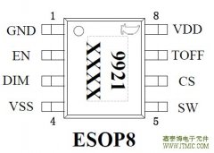 JTM9921 是一款高效率,稳
人气:201
JTM9921 是一款高效率,稳
人气:201
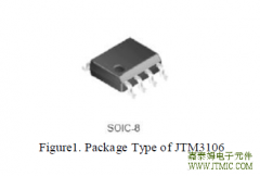 The JTM3106 is a 380 KHz fixed
人气:197
The JTM3106 is a 380 KHz fixed
人气:197
 The JTM1483,JTM1483A is a synch
人气:190
The JTM1483,JTM1483A is a synch
人气:190
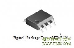 The JTM3501 is a 150 KHz fixed
人气:190
The JTM3501 is a 150 KHz fixed
人气:190
 粤ICP备13004986号-3