


目录
一,产品概述(General Description)
The JTM3440 is high efficiency, fixed frequency,Buck-Boost DC/DC converter that operates from input voltages above, below or equal to the output voltage. The devices are suitable for single lithium-ion, multicell alkaline or NiMH applications
where the output voltage is within the battery voltage range.The switching frequencies up to 1.5 MHz could befixed by employing an external resistor, and the
oscillator could be synchronized to an external clock. The quiescent current is 1mA, and this feature maximizing the battery life in portable applications.Other features include a 1µA shutdown, thermal shutdown and current limit. The JTM3440 is available in the 10-pin thermally enhanced MSOP packages (or upon request).
二.产品特点(Features)
Synchronous Rectification: Up to 95% Efficiency
Single Inductor
Fixed Frequency Operation with Battery
Voltages Above, Below or Equal to the Output
Quiescent Current 1mA (50uA low power mode: mode pin high)
Up to 1A Continuous Output Current
2.7V to 5.5V Input and Output Voltage range
Programmable oscillator frequency from 350kHz to 1.5MHz
No Schottky Diodes required VOUT<4.3V
VOUT Disconnected from VIN During Shutdown
1µA Shutdown Current
Package: Small Thermally Enhanced 10-pin MSOP
三,应用范围 (Applications)
Handheld Instruments
MP3/MP4 Players
Palmtop computers
Digital Cameras
四.下载产品资料PDF文档
 |
JTM3440 |
五,产品封装图 (Package)
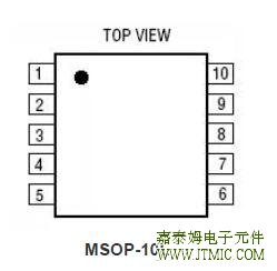
|
PIN NUMBER MSOP-10L |
PIN NAME | FUNCTION |
| 1 | RT |
Program the Oscillator Frequency |
| 2 |
MODE/SYN C |
Synchronization of the Internal Oscillator |
| 3 | SW1 | Switch 1 |
| 4 | SW2 | Switch 2 |
| 5 | GND | Ground |
| 6 | VOUT | Output |
| 7 | VIN | Input |
| 8 | EN |
ON/OFF Control (High Enable) |
| 9 | FB | Feedback |
| 10 | VC | Error Amp Output |
六.电路原理图
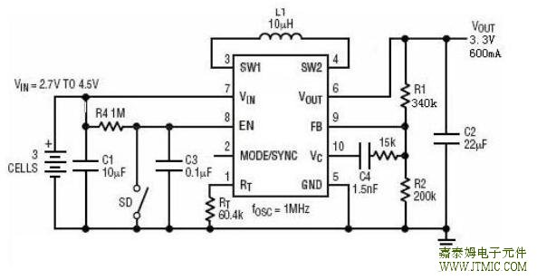
七,功能概述
The JTM3440 provides high efficiency, low noise power for applications such as portable instrumentation.
The JTM3440 allows input voltages above, below or equal to the output voltage by properly phasing the
output switches. The error amp output voltage on the VC pin determines the output duty cycle of the
switches.
Since the VC pin is a filtered signal, it provides rejection of frequencies from well below the switching
frequency. The low RDS(ON), low gate charge synchronous switches provide high frequency pulse width
modulation control at high efficiency.
八,相关产品
| 双路同步DC-DC降压IC | |||||||||||
| 型号 | 输入耐压 | 输出电压 | 输出电流 | 反馈电压 | 工作频率 | 效率 | 静态工作电流 | 待机电流 | 封装 | 直接替换 | |
| JTM8021 | 3.0V-6.0V | 双路可调 | 1.5A | 0.6V | 1.5MHz | 90% | 10uA | ESOP-8 | SY8021/L | ||
| JTM8022 | 2.3V-6.0V | 双路可调 | 2A | 0.6V | 1.5MHz | 90% | 150uA | 0.1uA | ESOP-8 | SY8022/L | |
| 同步DC-DC升降压IC. | |||||||||||
| 型号 | 工作模式 | 工作电压范围 | 输出电压 | 反馈电压 | 输出电流 | 效率 | 静态电流 | 工作频率 | 封装 | 直接替代型号 | |
| JTM3440 | PWM | 2.2V-5.5V | 可调 | 1.2V | 0.7A | 95% | 50uA | 1.15MHz | MSOP-10 | LTC3440/TPS61070 | |
| DC-DC升降压IC | |||||||||||
| 型号 | 工作模式 | 工作电压 | 输出 | 输出电压 | 输出电压 | 内置MOS | 效率 | 静态 | 工作频率 | 封装 | 直接替代型号 |
| 范围 | 电压 | 形式 | 精度 | 最大输出 | 电流 | ||||||
| 电流 | |||||||||||
| JTM6297 | PWM | 3.6V-26V | 最大60V | 可调输出 | ±2% | 2A | 90% | 70uA | 400KHz | SOP-8 | |
| JTM6298 | PWM | 3.6V-36V | 最大60V | 可调输出 | ±2% | 3A | 92% | 70uA | 400KHz | TO252-5L | |
| JTM6299 | PWM | 5V-45V | 最大60V | 可调输出 | ±2% | 5A | 94% | 70uA | 220KHz | TO263-5L | |
| 型号 | 工作电压 | 电流限制 | 静态电流 | 截止电流 | 内阻 | 欠压锁定电压 | 抗静电电压 | 响应时间 | 封装 | 替代型号 | |
| JTM4610H/L | 2.4V-5.5V | 1A可调 | 15uA | 1uA | 80 moJTM | 1.8V | 2 KV | 2 uS | SOT-25 | AAT4610/SY6280/LPW5202/6/ | |
| EUP3510/1TCS9107/TT9107 | |||||||||||
| UP7534/TT9707/TCS9607 | |||||||||||
| JTM9703 | 2.0V-6.5V | 2.1A可调 | 40uA | 1uA | 70 moJTM | 1.7V | 8 KV | 4.6 mS | SOT-25 | AAT4610/SY6280/LPW5202/6 | |
| EUP3510/1/TCS9107/TT9107/ | |||||||||||
| UP7534/TT9707/TCS9607 | |||||||||||
| JTM9701 | 2.2V-6.0V | 1.1A | 23uA | 0.1uA | 100 moJTM | 1.8V | 6KV | 400uS | SOT-25 | RT9701 | |
| JTM9715A/C/D | 2.5V-5.5V | 2.1A/1.0A | 25uA | 0.1uA | 80 moJTM | 1.7V | 4 KV | 400 uS | SOT-25 | RT9715 | |
| 0.65A | |||||||||||
| JTM9711A | 2.5V-5.5V | 2.1A | 25uA | 0.1uA | 80 moJTM | 1.7V | 4 KV | 400 uS | SOT-25 | RT9711 | |
 JTM4103是一款降压恒流型
人气:255
JTM4103是一款降压恒流型
人气:255
 JTM6286,JTM6285 采用 60V 高压
人气:213
JTM6286,JTM6285 采用 60V 高压
人气:213
 The JTM6297,JTM6298,JTM6299 reg
人气:210
The JTM6297,JTM6298,JTM6299 reg
人气:210
 外驱MOSOS管,PSR控制模式,
人气:208
外驱MOSOS管,PSR控制模式,
人气:208
 The JTM1542 is a compact, high
人气:207
The JTM1542 is a compact, high
人气:207
 户外LED照明解决方案,通过
人气:204
户外LED照明解决方案,通过
人气:204
 JTM9921 是一款高效率,稳
人气:201
JTM9921 是一款高效率,稳
人气:201
 The JTM3106 is a 380 KHz fixed
人气:197
The JTM3106 is a 380 KHz fixed
人气:197
 The JTM1483,JTM1483A is a synch
人气:190
The JTM1483,JTM1483A is a synch
人气:190
 The JTM3501 is a 150 KHz fixed
人气:190
The JTM3501 is a 150 KHz fixed
人气:190