


目录
一,产品概述(General Description)
The JTM6230 is a high performance positive voltage regulator designed for use in applications requiring very low Input voltage and very low dropout voltage at up to 3 amps. It operates with a VIN as low as 1.6V and VPP voltage 5V with output voltage programmable as low as 0.8V. The JTM6230 features ultra low dropout, ideal for applications where VOUT Additionally, the JTM6230 is very close to VIN. has an enable pin to further reduce power dissipation while shutdown. The provides excellent regulation over variations in line, load and temperature. The JTM6230 provides a power OK signal to indicate if the voltage level of VO reaches 92% of its rating value.
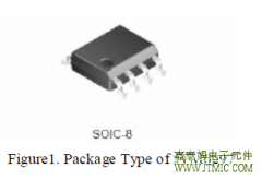
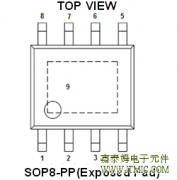
The JTM6230 is available in the power SOP-8PP pack-age. It is available with 1.2V, 1.5V, 1.8V and 2.5V in-ternally preset outputs that are also adjustable using external resistors.
二.产品特点(Features)
Adjustable Output Low to 0.8V
Input Voltage as Low as 1.6V and VPP Voltage 5V
240mV Dropout @ 3A
Over Current and Over Temperature Protection
Enable Pin
Low Reverse Leakage (Output to Input )
Power SOP8 –PP Packages with Thermal Pad
±2% Output Voltage
VO Power OK Signal
1.2V, 1.5V, 1.8V, 2.5V Options and Adjustable
Externally Using Resistors
VO Pull Low Resistance when Disable
三,应用范围 (Applications)
Motherboards
Peripheral Cards
Network CardsPeripheral Cards
Set Top Boxes
Notebook Computers
四.下载产品资料PDF文档
 |
JTM6230 |
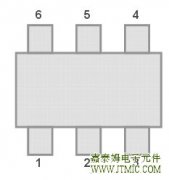
五,产品封装图 (Package)
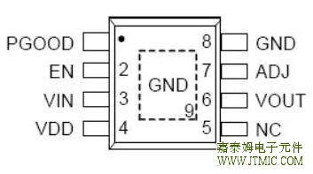
| PIN | NAME | |
| 1 | PGOOD |
Assert high once VO reaches 92% of its rating voltage. Open-drain output. |
| 2 | EN | Enable Input. (Active High) |
| 3 | VIN |
Input voltage. Large bulk capacitance should be placed closely to this pin. A 10µF ceramic capacitor is recommended at this pin. |
| 4 | VDD | Input voltage for controlling circuit. |
| 5 | NC | Not connected. |
| 6 | VOUT |
The power output of the device. A pull low resistance exists when deactivate device by VEN. |
| 7 | ADJ |
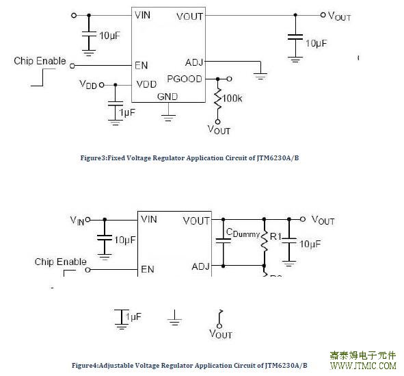
This pin, JTM6230A/B when grounded, sets the output voltage by the internal feedback resistors.If external feedback resistors are used, the output voltage will be VO = 0.8(R1+R2)/R2 Volts. |
| 8 | GND | Reference ground. |
六.电路原理图
七,功能概述
PowerOnReset
A Power-On-Reset (POR) circuit monitors both of supply voltages on VCNTL and VIN pins to prevent wrong logic
controls. The POR function initiates a soft-start process after both of the supply voltages exceed their rising POR
voltage thresholds during powering on. The POR function also pulls low the POK voltage regardless of the
output status when one of the supply voltages falls below its falling POR voltage threshold.
Internal SoftStart
An internal soft-start function controls rise rate of the output voltage to limit the current surge during start-up.
The typical soft-start interval is about 0.6ms.
Output Voltage Regulation
An error amplifier working with a temperature compensated 0.8V reference and an output NMOS regulates output to the preset voltage. The error amplifier is designed with high bandwidth and DC gain provides very fast transient response and less load regulation. It compares the reference with the feedback voltage and amplifies the difference to drive the output NMOS which provides load current from VIN to VOUT.
CurrentLimit Protection
The JTM6230 monitors the current flowing through the output NMOS and limits the maximum current to prevent
load and JTM6230 from damages during current overload conditions.
Short CurrentLimit Protection
The short current-limit function reduces the current-limit level down to 0.8A (typical) when the voltage on FB pin
falls below 0.2V (typical) during current overload or shortcircuit conditions.The short current-limit function is disabled for successful start-up during soft-start.
Thermal Shutdown
A thermal shutdown circuit limits the junction temperature of JTM6230. When the junction temperature
exceeds +170 ºC, a thermal sensor turns off the output NMOS, allowing the device to cool down. The regulator
regulates the output again through initiation of a new soft-start process after the junction temperature cools by
50oC, resulting in a pulsed output during continuous thermal overload conditions. The thermal shutdown is
designed with a 50 ºC hysteresis to lower the average junction temperature during continuous thermal overload
conditions, extending lifetime of the device.For normal operation, the device power dissipation should be externally limited so that junction temperatures will not exceed +125 ºC.
Enable Control
The JTM6230A/B has a dedicated enable pin (EN).JTM6230A:A logic low signal applied to this pin shuts down the output. Following a shutdown, a logic high signal re-enables the output through initiation of a new soft-start cycle. When left open, this pin is pulled up by an internal current source (5ìA typical) to enable normal operation. It’s not necessary to use an external transistor
八,相关产品
| LDO IC | |||||||||||
| 型号 | 最大输 | 输入电压 | 输出电压 | 精度 | 功耗 | 负载 | 线性 | 封装形式 | 状态 | 替代型号 | |
| 出电流 | 稳定率 | 稳定率 | |||||||||
| JTM6206 | 300mA | 7.0V | 1.2/1.5/1.8/2.0/2.1/2.2 | 2% | 7uA | 40-80mV | 0.05% | SOT-23 | 量产 | XC6206 | |
| 2.5/2.8/3.0/3.3/3.6/5.0V | SOT-23-3L | RT9166 | |||||||||
| SOT-89 | RT9169 | ||||||||||
| AIC1734 | |||||||||||
| AIC1722 | |||||||||||
| JTM6214 | 500mA | 8.0V | 1.8/2.5/2.8/3.0/3.3/ | 2% | 5uA | 12-30mV | 0.05% | SOT-89 | 量产 | XC6214 | |
| 3.6/4.2/5.0V | APL5885 | ||||||||||
| 带使能LDO IC | |||||||||||
| 型号 | 最大输 | 输入电压 | 输出电压 | 精度 | 功耗 | 负载 | 线性 | 封装形式 | 状态 | 替代型号 | |
| 出电流 | 稳定率 | 稳定率 | |||||||||
| JTM1134 | 500mA | 6.5V | 1.2/1.5/1.8/2.5/ | 2% | 静态电流:40uA | 0.6% | 0.4% | SOT-25 | 量产 | XC6204B/ | |
| 2.8/3.0/3.3/5.0V | 关断电流:1uA | XC6219B/ | |||||||||
| XC6221/ | |||||||||||
| RT9167/ | |||||||||||
| AIC1742/ | |||||||||||
| RT9193/ | |||||||||||
| LP2985/ | |||||||||||
| PT5107 | |||||||||||
| JTM6219 | 300mA | 6.5V | 1.2/1.5/1.8/2.5/ | 2% | 静态电流:25uA | 65dB | 0.20% | SOT-25 | 量产 | XC6219B/ | |
| 2.8/3.0/3.3/3.6V | 关断电流:1uA | XC6221/ | |||||||||
| JTM6210 | 700mA | 8.0V | 1.2/1.8/2.5/2.8 | 2% | 静态电流:30uA | 15mV | 0.01% | SOT-25 | 量产 | XC6210 | |
| 3.0/3.3/3.6V | 关断电流:1uA | SOT-89-5L | |||||||||
| JTM6230 | 3A | 6.0V | 0.8-VIN | 2% | 10uA | 0.10% | 0.20% | ESOP8 | 量产 | ME966/A | |
| APL5930 | |||||||||||
| APL5920 | |||||||||||
| RT9018 | |||||||||||
| RT9025 | |||||||||||
| 双路带使能LDO IC | |||||||||||
| 型号 | 最大输 | 输入电压 | 输出电压 | 精度 | 功耗 | 负载 | 线性 | 封装形式 | 状态 | 替代型号 | |
| 出电流 | 稳定率 | 稳定率 | |||||||||
| JTM6401 | 300mA | 10V | 1.8+2.8/1.8+3.3/ | 2% | 静态电流:25uA | 50mV | 0.01% | SOT-26 | 量产 | XC6401/ | |
| 2.8+3.3/2.8+1.8V | 关断电流:0.11uA | PT5127/ | |||||||||
| EUP7201/ | |||||||||||
| AP6401/1 | |||||||||||
| SGM2207 | |||||||||||
| JTM9182 | 300mA | 10V | 2.8+1.8/3.3+1.8/ | 2% | 静态电流:25uA | 50mV | 0.01% | SOT-26 | 量产 | RT9182/ | |
| 1.8+2.8V | 关断电流:0.11uA | RT9011/ | |||||||||
| PT5128 | |||||||||||
| 可调输出LDO IC | |||||||||||
| 型号 | 最大输 | 输入电压 | 输出电压 | 精度 | 功耗 | 负载 | 线性 | 封装形式 | 状态 | 替代型号 | |
| 出电流 | 稳定率 | 稳定率 | |||||||||
| JTM6205 | 300mA | 6.0V | 可调,最低0.9V | ±2% | 静态电流:57uA | 50mV | 0.1% | SOT-25 | 量产 | AP2127 | |
| 关断电流:1uA | AP2128 | ||||||||||
| PAM3103 | |||||||||||
| SGM2019 | |||||||||||
| JTM6215 | 500mA | 6.0V | 可调,最低0.8V | ±1.5% | 静态电流:40uA | 0.60% | 0.08% | SOT-25 | 量产 | AP2127/8 | |
| 我司的JTM6204BXX2MR/SOT-25有如下优点: | |||||||||||
| 1.最大可达300mA负载电流,耐电流可达500mA. | |||||||||||
| 2.工作电压2.5-6.5V,耐压可达7V. | |||||||||||
| 3.静态电流小,压差小,纹波小,带载能力和抗干扰能力强。 | |||||||||||
| 4.可广泛用于手机/MID/MP3&MP4&MP5/蓝牙/数码相机/GPS/点读笔/音响/液晶电视/电表/电子钟表/电子玩具等各类电子产品市场。 | |||||||||||
| 5.目前我司产品有出在三星/LG等著名品牌的手机产品上的(手机的要求是比较高的),在带载能力、纹波、静态电流、抗干扰、压差等各方面参数都要优于目前市场上国内同类产品的。目前市场上很多国内同类产品是进不了手机市场的,性能参数达不到要求的。 | |||||||||||
| 产品应用: | |||||||||||
| 1.MP3/MP4/MP5/PMP 播放器 | |||||||||||
| 2.MID/UMPC | |||||||||||
| 3.GPS/行驶记录仪 | |||||||||||
| 4.PDVD/车载DVD/汽车音响 | |||||||||||
| 5.液晶电视/液晶显示器 | |||||||||||
| 6.移动电源/电子烟 | |||||||||||
| 7.小家电、家电控制板 | |||||||||||
 JTM4103是一款降压恒流型
人气:255
JTM4103是一款降压恒流型
人气:255
 JTM6286,JTM6285 采用 60V 高压
人气:213
JTM6286,JTM6285 采用 60V 高压
人气:213
 The JTM6297,JTM6298,JTM6299 reg
人气:210
The JTM6297,JTM6298,JTM6299 reg
人气:210
 外驱MOSOS管,PSR控制模式,
人气:208
外驱MOSOS管,PSR控制模式,
人气:208
 The JTM1542 is a compact, high
人气:207
The JTM1542 is a compact, high
人气:207
 户外LED照明解决方案,通过
人气:204
户外LED照明解决方案,通过
人气:204
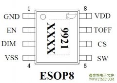 JTM9921 是一款高效率,稳
人气:201
JTM9921 是一款高效率,稳
人气:201
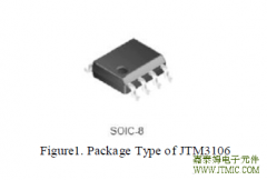 The JTM3106 is a 380 KHz fixed
人气:197
The JTM3106 is a 380 KHz fixed
人气:197
 The JTM1483,JTM1483A is a synch
人气:190
The JTM1483,JTM1483A is a synch
人气:190
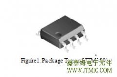 The JTM3501 is a 150 KHz fixed
人气:190
The JTM3501 is a 150 KHz fixed
人气:190
 粤ICP备13004986号-3